This thread has been locked.

If you have a related question, please click the "Ask a related question" button in the top right corner. The newly created question will be automatically linked to this question.

ADS1018-Q1: ADS1018-Q1

Part Number: ADS1018-Q1
Other Parts Discussed in Thread: ADS1018

Hi

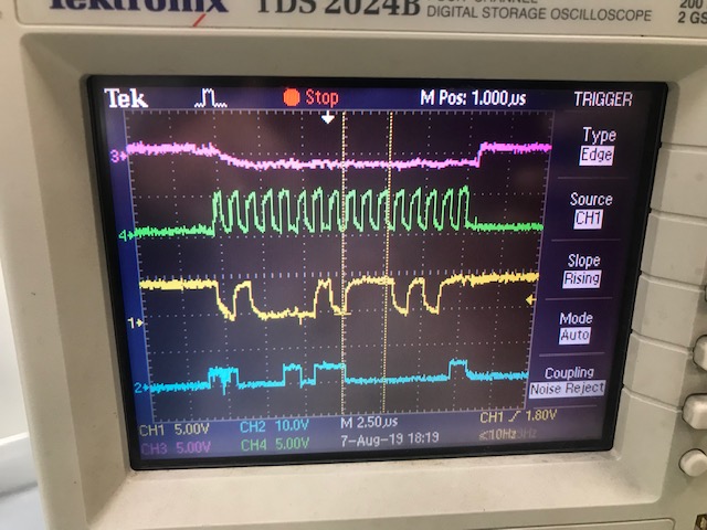
i am using ads 1018 adc on mpc5777xc controller, i unable to get adc data , just getting 255 value, please tell me about DRDY pin , is it require to monitor or not , and how many times need to send data to config reg

thanks

  • Avanti,


    There are a couple of things that could be happening, but I would start by plotting the SPI communication with an oscilloscope or logic analyzer. It is important to see how the device is responding to the /CS line.

    The default setting of the device when power is applied to VDD, is to be in power-down/single-shot conversion mode. After this you will need to either set the device to continuous conversion mode to start the ADC or start a conversion by writing a 1 into bit 15 of the Config Register. After that, you should be able to read from the device after the ADC completes it's first conversion.

    Are you able to read the conversion register using the 32-bit data transmission cycle? What is your input voltage and what data do you get out? I would note that 255 is FF, and this device is a 12-bit device. It outputs 12 bits right justified, with LSBs zero padded.

    In your next post, outline the commands that you're sending to the ADC, and then show the plots of the communication.


    Joseph Wu

  • Hi joseph,

    firstly thanks for your reply.

    i have initiated SPI Communication, check all the signals on oscilloscopes, 

    my configuration is like this

    1. initialization of SPI

    2.sending data to ADS, Means setting config register, sending 58EB like 

    write(0x58EB) IN WHILE LOOP. 

    SS=0

    MUX=100

    PGA  001 MEANS UTP 4 V

    MODE= CONTINUOUS

    data rate -3330sps

    TS= adc mode

    pull up enable =1

    nop 01

    0

    sending this data in while 1

    after minor delay ..reading data of spi then getting 255

    if data ready==0

    then read data fuction , as mentioned in data sheet if data ready pin is low then our data is ready,.

    please tell me what changes i need to do here. and i am usinh 1 mhz spi clock frequency.

    thanks in advance.

  • Avanti,


    As I mentioned previously, I'd like to see the scope shots of the SPI communication. You will want to look at the plots for /CS, DIN, DOUT, and SCLK to make sure that the device is communicating properly. Once you get the scope shots post them back here.

    Also, I would recommend using the 32-bit data transmission cycle as shown in Figure 13 of the datasheet. Using this communication, you will be able to see both the output data and the configuration register. Your plot should look like the figure.

    Just to check, if you are in continuous conversion mode, even if you are not reading the device back, you should be able to see a periodic pulse on the DOUT/DRDY line at the data rate. You would need to keep /CS low for that entire time.


    Joseph Wu

  • Hello joseph,

    i checked the data on oscilloscope, now i am getting some value, ani after decreasing or increasing pot , value also changes.

    now i want read the 2 s configure data into decimal form,

    i am reading data in 8 bit register.

    please tell me the way of reading data.

    thanks a lot in advance

  • Hi joseph,

    please tell me how to read the 2s complement data .

    and after what time need to read it

  • Hi joseph,

    please tell me how to read exact data , and convert it into decimal,its very urgent . please help me for this.

    thanks in advance

  • Avanti,


    You should be able to convert the output digital code based on the Data Format section of the datasheet on page 16.

    The ADC will give an output code of 2 bytes to correspond to a 16-bit number. However, the last four bits should be 0 and truncated. This will yield a 12-bit number in 2's complement notation. Here is how you get the conversion data:

    1. Get the 16-bit data.
    2. Remove the last four bits of 0 to get 12-bit data
    3. Convert this Hexadecimal result to decimal.
    4a. If decimal number < 2048, then this is the Result,
    4b. If decimal number > 2047, then the Result=(decimal number - 2^12)
    5. Measured voltage = (Result/2^11)*(positive FSR). That means that if the FSR=±2.048, positive FSR=2.048.

    It's often easy to put this together in an excel spreadsheet, any you can try this with several test values.

    If you're having problems reading data because of the SPI communications, can you post the SPI communications that you see with the oscilloscope?


    Joseph Wu

  • Thank you so muvh joseph for your reply actually now the problem is ..i am trying to read data in 16 bit trasmission format ..but as mentioned in datasheet i have to take cs higg aftetr 16 th clock pulse..it us creating problem for me...so please explain me how to monitor cs line for accurate data...and also if i am using 32 bit datatransmission then last two bytes i am getting is as it is data config.means if i am sending 42 eb ..the n i should get last 2 byte 42 eb ...this is true ...?but i am not getting last two byte 42eb as checked on dso
  • Avanti,


    If you are using the 16-bit transmission format, you shouldn't need to monitor the /CS line. The /CS line is used only as a chip select to determine which SPI device the master wants to talk to. If you are only using one SPI device, you may not need to even use the /CS and could potentially tie this low.

    The line you need to monitor is the DOUT/DRDY line. The transition of this line low indicates that the device has completed a conversion and that data can be read out. Generally, it is best to use this device as an interrupt. If you wait too long to read the data after a conversion completes. The data readout may be interrupted by a new data as the next conversion completes. The ADC does not stop a new data from coming out if a new conversion is ready.

    If you are having problems with the 32-bit data transmission cycle, what error are you getting for the read out? Can you show this in the oscilloscope shot? I would note there are two possible errors that I can think of.

    First if you are in the process of reading out the 32-bits and a new conversion completes, the DOUT/DRDY register immediately is updated with the new ADC data. This interrupts your original read. Second, the configuration register may not be updated immediately. When you set the configuration register, I believe the device completes the conversion in progress and updates the configuration register after the conversion. If you are writing the configuration register, and immediately read the register, then you may be reading the previous configuration register setting.


    Joseph Wu

  • Hi joseph,

    i am facing one problem regarding cs line, 

    for 16 bit transmiision as mentioned in datasheet, we have to make cs high after 16 th cloclk pulse, if i am doing this , then cs not runs properly means it is getting high in betwwen middle of 16th clock pulse ,

    so please explain hoe to control cs .

  • Avanti,


    Can you show what is happening with a oscilloscope shot of the communications? For the /CS line, it should stay low through the entire communication transmission. If the /CS goes high before all the SCLK pulses come through, this is not a problem with the device, this is a problem with programming the microcontroller.

    Regardless, post the SPI communication (all lines /CS, DIN, DOUT, SCLK) and we can discuss the problem.


    Joseph Wu

  • Avanti,


    I haven't heard from you for a while, so I thought I'd check to see if you've solved your communications problem with the ADS1018.

    We had covered a couple of different problems with the SPI, but at the last post, I had asked for a scope shot for your communications to better understand your problem with the /CS line.

    Hopefully, you were able to solve this problem and I'll close this post for now. However, if you haven't solved the communications issue, post back and we'll continue to work on this thread.


    Joseph Wu

  • HI ,

    Can you please tell me, how to extract main data from raw data,means want to know about resolution.

  • Avanti,


    The conversion of the data from the ADC is described in the datasheet in the Data Format section on page 17. The data is put in binary twos complement format that is left justified within the 16-bit data word. A positive full-scale (+FS) input produces an output code of 7FF0h and a negative full-scale (–FS) input produces an output code of 8000h. The data comes in from SPI on the falling edge of the SCLK. When I asked about the raw data, I wanted to know about what that 16-bit number is, and what FSR you are using.

    As I mentioned in a previous post, I'd like to see the communication from the ADC with an oscilloscope. I've already given an outline as to how to make the conversion. However, it might be easier if you showed a plot of a scope shot, with the SCLK, DIN, DOUT and /DRDY. With that, we could look at the resulting data and show the conversion.


    Joseph Wu

  • hi joseph,

    u have defined how to convert data  into voltage, these above all stages have 2s complement conversion step also.

  • hi joseph,

    i am sending 0x421B , THIS 16 BIT VALUE TO ADC,them immediately reading data,

    below is my code

    my FSR is 4.096

    DSPI_B.PUSHR.PUSHR.R = (uint32_t)((uint32_t)(cmd<<16) + data);
    DSPI_B.SR.B.TXRXS = 1;
    response = DSPI_B.POPR.R;

    i am reading data from pop register, 

    i am attaching my dso data, first one is cs, clock ,and data in to adc,  and last one data out from adc.

    due to probe prblem it is little bulky,

    and i am not getting any constat data value, continuosly it is changing,

    please tell me after what time i should read data?

    thank you so much for in advance


  • Avanti,


    There are a couple of things that could be going on here.

    Sending 0x421B means that you're using the device in temp sensor mode. This is probably a good mode to look at because you're probably expecting a value near 0x0C80 if the device is near room temperature. You can compare that value with what you're reading.

    Looking at the scope shot, and based on your comments:
    Red = /CS
    Green = SCLK
    Yellow = DIN
    Blue = DOUT

    Now here are the problems that I see with the scope shot. First, there's a lot of noise. It's possible that you're getting some bad values because of that, and noise on SCLK could cause the device to clock out data when the device shouldn't. I would definitely clean that up. Second there are some rounded edges to the clock lines. I'm not sure that's necessarily a problem, but I was expecting to see cleaner square waves. Third, there is something wrong with /CS. The CS line should be from 0V to 5V like the other digital lines. However, it looks like /CS is going ±2V or so above and below the ground based on the oscilloscope. However, it does look like the device is responding at the correct time. DOUT rises at about the time I would have expected when /CS would have started going low. It also rises at the correct time.

    If the yellow line is DIN, then you're not sending 0x421B. To me, that looks like 0x42EB. That would mean that you're reading one of the inputs at a different data rate. I'm unsure because the register DR[2:0]=111 should not be used.

    I would check all your connections. If you have problems with this, send a schematic and maybe a photo of your setup.

    When it comes to reading the data, you shouldn't read the device completely asynchronously. If the device is being used in continuous conversion mode, the device is giving new data at the data rate. You would wait until DOUT/DRDY goes low, and then send the SCLKs to read the data. However, If you wait too long, then the new data could interrupt a read in progress. The DOUT register would be updated mid-read and corrupt the output data.

    If you are programming the device, you need to wait for the device to set the configuration, and then wait for the data period for the conversion to complete. If you set the device to 128SPS, then you would need to wait 1/128 seconds (+10% for oscillator clock variation). That would be about 8.6ms if you set the conversion just as the conversion in progress is about to complete.

    Note that if you are in continuous conversion mode, then this time would be as much as 2x longer. If you program the configuration register, the configuration register isn't set until after the conversion in progress completes. If you set the configuration register just as a new conversion started, then the data from the new configuration won't be ready for two conversion periods.


    Joseph Wu

  • Hi joseph,

    i want to understand the above steps

    the step 4a  and 4b ..i am not getting  these steps. please explain me.

    one more question .. at what stage i will get the full count 4096.

  • hi joseph,

    my vref is 5v and my pot max voltage is 3.5v

    when i remove last 4 bits from data .i am getting 1160 value ,this is 12 bit value .

    so this is  wrong or right , i am not getting, and how to proceed again this value to main data.

  • Avanti,


    First, have you been able to clean up the digital signals that you see with the oscilloscope? I was concerned that you might be getting digital errors in your communications. Second, can you send a schematic? It would help debugging of what you are measuring. If you have some sort of voltage divider from a potentiometer and a resistor, it would be good to have those values too.

    Looking at your result, this may be correct, but you might be in the wrong range. For example, if you are in the ±6.144V FSR, and you are measuring 3.5V. Then you might get:

    (3.5V/6.144V)*2^11 = 1167 (This would be 48Fh)

    This code is close to the 1160 that you are seeing. Note that if were on the ±4.096V FSR, this value would be different. You would see:

    (3.5V/4.096V)*2^11 = 1750 (This would be 6D6h)

    Because of the 2s complement notation the highest positive value would be 7FFh or a code of 2047.


    Joseph Wu

  • Hi joseph,

    today i have multiple questions. i have below doubts.

    my FSR is 6.144

    pot max voltage is 3.5

    1. first thing please tell me we are getting 16 bit value , so last four bits should be 0 or it will read.

    for  3.008 v

    when i am reading pop register its value is A90 IN HEX, and 2704 in decimal

    if i remove last four bits then it is A9 means 169 value.this value is constant at any time,but if my pot voltage decreases from 3.008 to 3.004 then i am getting 589 value ,due to little fluctuation . lots of difference in count

    1.FSR =6.144 INPUT VOLTAGE 3.008 , DATA=169 IN DECIMAL(12 BIT)

    2. FSR =6.144 INPUT VOLTAGE =3.004 DATA =585 IN DECIMAL(12 BIT)

    HOW IT IS COMING PLEASE EXPLAIN ME

    2 . ANOTHER IS in datasheet it is written that data will be in binary 2s complement form.

    so the above data is in 2s complement or final data.

    i am not understanding the data i am getting is in normal or 2s complement so need to convert it?? or not

    please please help me for this,

    thanks a lot in advance.

  • 1.FSR =6.144 INPUT VOLTAGE 3.506 , DATA=1316 IN DECIMAL(12 BIT)

    this above data 1316 is in which format.

  • ip voltage FSR 12 bit data
    3.506 6.144 1316
    2.986 6.144 681
    2.492 6.144 576
    2.053 6.144 3364
    1.492 6.144 2372

    these are above reading.please help me for this.

  • Hi joseph,

    today i am not asking any doubt.

    Thanks you so much for your help and guidence, my adc is working properly and getting exact output. 

    you guide me very properly. thanks for your valuable time and help.