


Part Number: DAC8560
Hi,
My design as below:
I want to control the MOS through DAC8560 to realize the current adjustment function.
Reference design on similar specifications.
I don't know if this design is feasible?
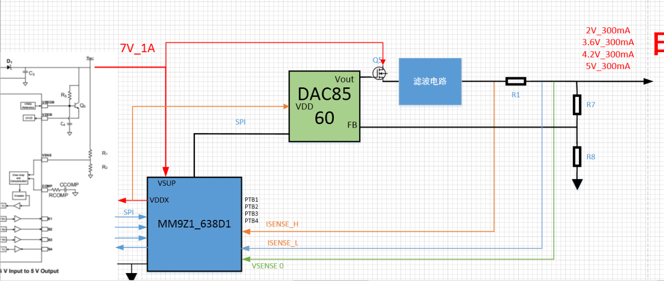
thanks.
Part Number: DAC8560
Hi,
My design as below:
I want to control the MOS through DAC8560 to realize the current adjustment function.
Reference design on similar specifications.
I don't know if this design is feasible?
thanks.
