This thread has been locked.

If you have a related question, please click the "Ask a related question" button in the top right corner. The newly created question will be automatically linked to this question.

DAC7578: DAC read sequence on input register

Part Number: DAC7578
Other Parts Discussed in Thread: DAC7678, DAC5578

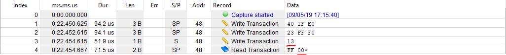
My team is using the DAC7578 12-bit, 8 channel device on a custom board. Prior to the custom board prototype, I have been using the DAC7678 EVM for development. I am experiencing some unexpected issues in the read sequence of the DAC7578. Please see the attached snapshots of the captured I2C byte sequences to the two devices.

DAC7578:

DAC7678:

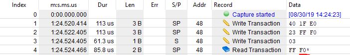
The test sequence on both devices is:

1. Power up all DAC channels (Power Down Register 0x40; PD1 = PD2 = 0; all channels selected)

2. Write full count to DAC Input register Channel D and update all DAC registers (Global Software LDAC: 0x20; Channel D: 0x03; Full count: 0xFFF)

3. Read back DAC input register D (0x03)

However the read-back from DAC7578 does not reflect the full count written to it, although the voltage on Channel D is observed correctly, at full reference value.

What is the difference between DAC input register and DAC register for each channel?

Which register should be read back in software?

What might be causing the discrepancy in the read back between the two devices?

  • Hello Ruta,

    Could you please describe the exact sequence of commands used to access the Channel D read-back? I'm not sure I'm interpreting the two screen captures correctly.

    There are also two read-back sequences described on page 32 of the datasheet, I think it would be interesting to try both to see if they are each reporting unexpected data.

  • Thanks for your reply Kevin,

    The sequence of commands has been captured using a I2C protocol analyzer and shows the byte data going over the bus. It is a nascent application, testing out the prototype board as power up-write channel-read back channel.

    For both devices:

    1. Power up all DAC channels 

    CA Byte: 0x40 (Power-down Register)

    MSDB+LSDB: 0x1F, 0xE) (PD1=PD2=0 for power-up; DAC A - DAC H bits set to 1, X bits set to 0)

    2. Write full count (FFF0) to DAC channel D

    CA Byte: 0x23 (Global software LDAC, write to channel D)

    MSDB+LSDB: 0xFF, 0xF0 (full count, expected analog output is observed on both DACs)

    3. Read the value written to channel D

    CA Byte: 0x03 (Read input register, channel D)

    4. Read bytes

    On DAC7678 this is 0xFFF0 as expected. On DAC7578 this is 0xFF00 even though the analog output is correct.

    Why the discrepancy on the DAC7578? On both of them I am only using an external reference of 3.3V, DAC7678's internal reference is disabled.

    Also I studied the read back sequence described in the operating example on P40 of the DAC7578 datasheet. I am following a similar read back sequence from Channel D (reading the input register). That's why I wanted to know what the difference is between the DAC register (CA byte 0x10) and Input register (CA Byte 0x00).

  • Hi Ruta,

    Have you tested this with the DAC register and observed the expected behavior?

    Most of our DAC products, especially the multi-channel devices, are designed with what is commonly referred to as a double-buffered shift register for the DAC data. This means that data is basically loaded to a temporary location until the LDAC signal is tripped either via a hardware pin, or in this case, a software command. I have seen some cases in which reading back the temporary buffer register could yield some unexpected results, but I cannot say for certain without digging more into this device specifically.

    I would be interested in seeing the results of reading the DAC data register as opposed to the input register as well as the results of the alternate readback method initiated by a repeated start with the R/W bit set to 1. This should repeat the previous write frame contents.

  • Hi Kevin, I tested this with the DAC register and I am still seeing the same issue.

    DAC7578 on custom board:

    DAC7678 EVM:

    I saw the start/repeated start read method. What is the command-access byte used in this case?

    Or is it expected to just send out START->slave address->repeated START->(receive data bytes)->NACK?

    Thanks for your help

  • Ruta,

    That is interesting - this was my lead consideration for how this read may have been corrupted.

    Yes - the alternate read method is just repeated start with the slave address and the R/W set high.

    Did you write any data to any of the other DAC channels?

  • Hi Kevin,

    Yes I have seen similar results while writing to the other channels on DAC7578. I just posted Channel D on this thread as one example.

    When I tried the alternate read method I did not receive a response from the device. I am still trying to debug if this was an error on my part, but the device does not appear to release the SDA line from the low position after sending the first start condition with the slave address.

  • Ruta,

    I have been out of office on travel for the last 2 weeks, trying to catch up on various topics now.

    I found another E2E thread (https://e2e.ti.com/support/data-converters/f/73/p/803228/2975424#pi320995=1) where another user appears to be reading from the device with no issue, though I have not played with this myself.

    Paul appeared to have a HW setup available from that thread, I will see he still has that setup to run any further tests to help on this topic.

    Meanwhile, perhaps it would be helpful to review your custom board schematic. The FAE supporting you has reached out to me via email, if you'd like to move support there to share the schematic etc. we can pursue that.

  • Hi Ruta,

    Can you confirm if the devices you have are actually DAC7578 and not DAC5578? The behavior you are describing is correct for a 8-bit device.  If you are not sure, please tell me all of the markings on the top of the device and I can confirm for you.

    Another quick test would be to try to measure a different between a few 12 bit codes.  For example:

    1. Write 0x8000 to a channel, measure and record the output

    2. Write 0x80F0 to the same channel, measure and record the output - did the output change from step 1?

    3. Write 0x8100 to the same channel, measure and record the output - has it changed now?

    If there is no change from 1 and 2, then you probably have a 8-bit device.  If you see only a change after step 3, then that confirms it. 

    Thanks,
    Paul

  • Paul, Kevin: I checked and there was actually a discrepancy on the BOM generated for the custom board manufacturer and they populated the wrong part (5578). Thank you so much for your help, and apologies since it was rather difficult to get hold of the actual part on the board.