This thread has been locked.

If you have a related question, please click the "Ask a related question" button in the top right corner. The newly created question will be automatically linked to this question.

DAC38RF82: JESD204B configuration

Part Number: DAC38RF82
Other Parts Discussed in Thread: DAC38RF89

hello,

We have a one JESD204B master implemented on a Xilinx FPGA (ULTRASCALE device).

In the FPGA configuration M=2, L=8 (LMFS).

Eight serdes lanes are connected to the DAC38RF82.

We have a 16bit/2.5Gbps mode in which four lanes are connected to DAC A in the DAC38RF82 and four lanes are connected to DAC B (ONE_DAC_ONLY=0, ONE_LINK_ONLY=1).

The physical connections are as follows:

FPGA                     DAC38RF82

TX0                        RX1

TX1                        RX4

TX2                        RX6

TX3                        RX7

TX4                        RX5

TX5                        RX0

TX6                        RX2

TX7                        RX3

 Polarity should be inverted (in the DAC) for TX0, TX2, TX5, TX7.

The JESD mode we use for the 16bit/2.5Gsps is LMFSHd=82121.

In the FPGA, TX0 uses lane ID=0, TX1 uses lane ID=1 and so on for the rest of the TXn.

FPGA TX0-TX3 are routed to DAC A of the device (via the cross-bar, lane enable, etc.).

FPGA TX4-TX7 are routed to DAC B of the device.


My questions:

  1. Using Table 9, JESD204B Formats for DAC38RF82 and DAC38RF89 (p. 30 in the datasheet):
    We use the mode in last table entry (41121 / 82121).
    It seems the mode we require is 2 TX, 82121.
    What is the difference between 1 TX and 2 TX? (we use ONE_DAC_ONLY=0, ONE_LINK_ONLY=1).
  2. Using Table 41, Register Programming for JESD and Interpolation Mode (p. 52 in the datasheet):
    Which mode is the correct one for us: 82121/NA or 41121/82121 ?
  3. Giving the above information, can you fill the enclosed (from DAC38RFxx EVM GUI):
    (or supply with the relevant registers settings)
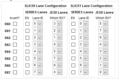
Thank you !

Gil Hershman

  • hello,

    I’ve made some progress with this issue.

    We found some errors in the mapping I wrote in the original post, so I am posting a corrected version:

    We have a one JESD204B master implemented on a Xilinx FPGA (ULTRASCALE device).

    Eight serdes lanes are connected to the DAC38RF82.

    We have a 16bit/2.5Gbps mode in which four lanes are connected to DAC A in the DAC38RF82 and four lanes are connected to DAC B (ONE_DAC_ONLY=0, ONE_LINK_ONLY=1).


    The physical connections are as follows:

    FPGA                     DAC38RF82

    TX0                        RX4

    TX1                        RX2

    TX2                        RX5

    TX3                        RX1

    TX4                        RX0

    TX5                        RX6

    TX6                        RX3

    TX7                        RX7


    Polarity should be inverted (in the DAC) for RX2, RX5, RX0, RX7.

    FPGA TX0-TX3 are routed to DAC A of the device while FPGA TX4-TX7 are routed to DAC B of the device.

    The FPGA JESD mode we use for the 16bit/2.5Gsps is LMFSHd=82121 (M=2, L=8).


    My questions:

    1. Using Table 9, JESD204B Formats for DAC38RF82 and DAC38RF89 (p. 30 in the datasheet):
      We use the mode in last table entry (41121 / 82121).
      It seems the mode we require is 2 TX, 82121.
      What is “1 TX” and “2 TX”? does it correspond to M?
    2. Using Table 41, Register Programming for JESD and Interpolation Mode (p. 52 in the datasheet):
      Two “82121” modes are there: 82121/NA and 41121/82121.
      It seems the correct mode for us is 41121/82121.
      In that mode, M=1 and L=4.
      What is the difference between both modes?
    3. I have two methods to fill the enclosed:
       Method 1 assumes multi-DUC2 expects RX0/6/3/7 on its first four lanes (0x25F, default lane_ID 0-3).
      Method 2 assumes multi-DUC2 expects RX0/6/3/7 on its last four lanes (0x260, default lane_ID 4-7).
      Which is correct?

      Initial Lane ID setting in the FPGA TX4-TX7 is 4-7. I suspect, because M=2 in the FPGA, the FPGA logic changes it to 0-3: TX4 = lane ID 0, TX5 = lane ID 1, etc.
      Which Lane IDs does multi-DUC2 expect?
      Is there a rule in the JESD204B that says that the Lane ID the DAC expects (per lane) should be the same as the JESD core sends (per that lane)?

    Thank you

    Gil

  • Hi,

    To add to the above:

    Is Method 3 a valid option?

    The first four lanes in multi-DUC2 change its Lane IDs to 4-7 and RX0/6/3/7 map to them.

     Thanks

    Gil

  • Hi Gil,

    We are looking into your question and will get back to you.

    Regards,

    Vijay

  • Gil,

    1 TX means one DAC output and 2 TX means 2 DAC outputs. In the 41121 case, there will only be one output from the device and this will use 4 lanes. For mode 82121, there will be two DAC outputs, each output using 4 lanes of input data.

    The main difference between these two modes is one uses one DUC and one DAC and the other uses two of each.

    Regards,

    Jim 

  • Hi Jim,

    Thank you !

    Can you please refer to my 3rd question?

    Assuming "82121, 2 TX" mode: which of the two (method 1 and method 2) is the correct one?

    Can you please also refer to this (in the 3rd question)?

    Initial Lane ID setting in the FPGA TX4-TX7 is 4-7. I suspect, because M=2 in the FPGA, the FPGA logic changes it to 0-3: TX4 = lane ID 0, TX5 = lane ID 1, etc.
    Which Lane IDs does multi-DUC2 expect?
    Is there a rule in the JESD204B that says that the Lane ID the DAC expects (per lane) should be the same as the JESD core sends (per that lane)?

    Thank you

    Gil

  • Gil,

    There is no rule regarding this. You can assign any lane ID to any lane.

    Regards,

    Jim

  • Hi Jim,

    I will clarify my question:

    multi-DUC2 has eight lane inputs. I am using four of those in "82121, 2 TX" mode.

    DAC38RF82 RX lanes 0, 3, 6, 7 map to those four multi-DUC2 inputs.

    1. These four multi-DUC2 inputs: Which register sets them up: 0x25F or 0x260? 

    2. You said method 3 works. Which of methods 1 and 2 will also work? (see the methods on previous post in this thread).

    3. Which lane-IDs does multi-DUC2 expect to see on these four inputs?

    Thanks

    Gil

  • Gil,

    I need to know how the other 4 lanes are routed to DUC1 before I can answer any of these questions. For DUC2, register 0x25F selects which RX input to use for the DUC. Register 0x024A enables these inputs. For your DUC2 setting, I think you will set 0x25F to 0x0367 and register 0x24A to 0xF001.

    Regards,

    Jim


  • Hi Jim,

    The routing for DUC1 is shown in the methods 1/2/3 pictures (same routing in the three methods pictures):

    DAC serdes 4/2/5/1 are routed to DUC1.

    So, 0x25F is used for routing of the four RX serdes to DUC2.

    Method 2 will not work (it uses the last four JESD lanes, register 0x260).

    Which of methods 1 or 3 is correct? (you tested method 3 and it works).

    The difference between them is the lane IDs.

    Which lane-IDs does multi-DUC2 expect to see on these four inputs?

    Thanks

    Gil

  • Gil,

    What you have shown in method 3 above is correct. The way the GUI works is the column labeled as "Which RX" uses the top row first and works its way down. This is a little confusing. The lane ID is correct as DUC2 uses the first four rows in this table and will use lane ID 4, 5, 6, and 7. The lane ID is not important as the DAC only uses this for ILA error reporting, which can be ignored.

    Regards,

    Jim    

  • Jim,

    One correction regarding 0x24A:

    Bits 15:8 refer to serdes lane enable. So, for DUC2 it should be 0x24A[15:8]=0xC9 .

    You can see the same field in DAC3xJ84 datasheet (page 86).

    Thanks

    Gil