Hi
I appreciate if you could anwer these two questions about DAC39J84.
1- In the DAC39J84 datasheet, Figure 75, it has been shown that for CLK and SYSREF interface using LVPECL signaling the AC coupling caps are located close to the DAC. However, in the evaluation board they are placed close to the CLK IC. Could you please let me know which configuration is correct?
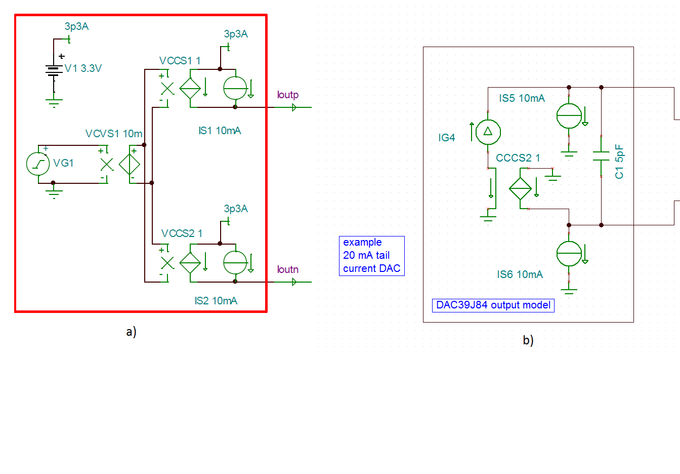
2- My understanding of DAC39J84 is that it is a current source, thus I used the model in figure(a) to model it in TINA, is this model correct? I asked this cause I recently posted a question about DAC39J84 output interface and for the answer I got Figure (b) as its model . I appreciate you help me here and confirm with me that model shown in Fig (a) is the correct one.
Regards
Samaneh