This thread has been locked.

If you have a related question, please click the "Ask a related question" button in the top right corner. The newly created question will be automatically linked to this question.

ADS8332: Read 0 for all channels

Part Number: ADS8332
Other Parts Discussed in Thread: REF3430, OPA320

Hello, we interfaced the ADS8332 with an LPC1857 (NXP) using the SSP0.

We can read/write the CFG register. The last attempt was made with the CFG written at 0x0F37.

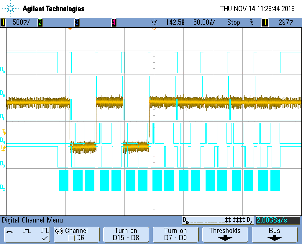
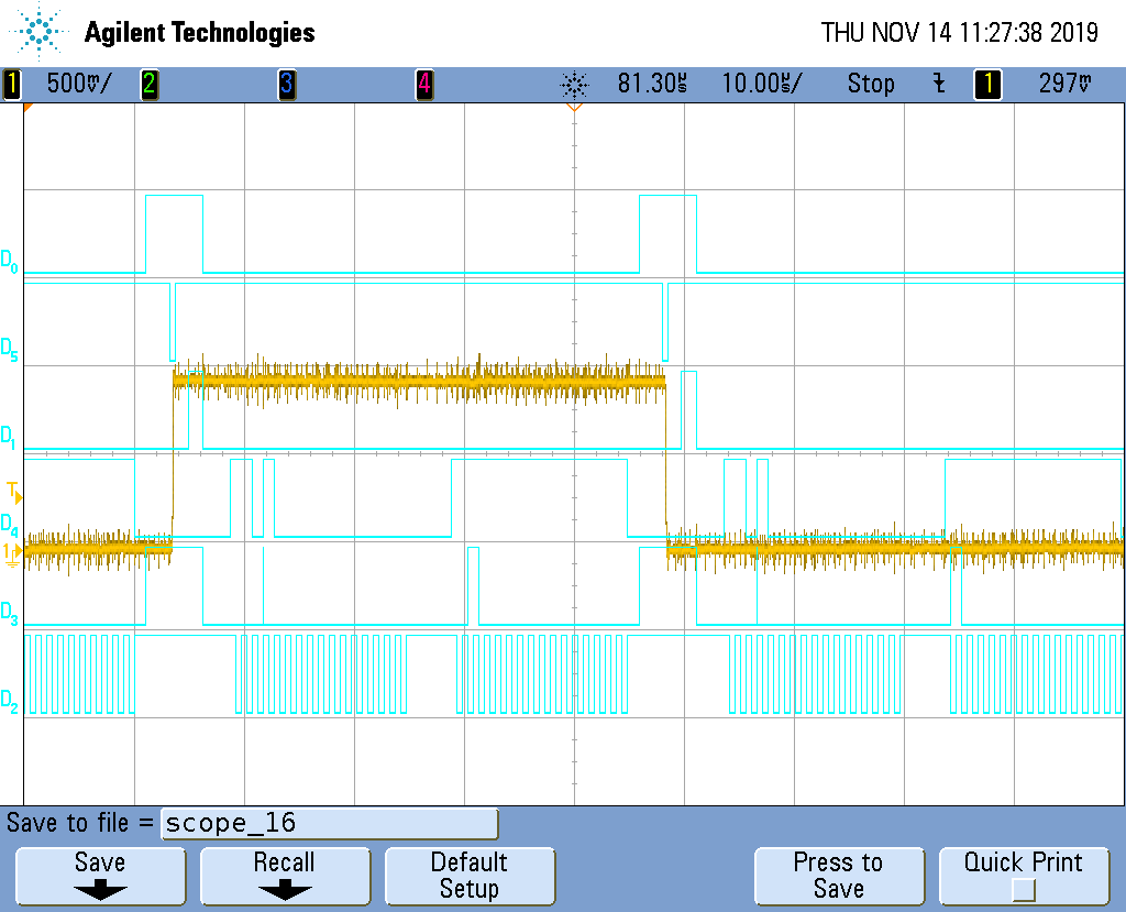
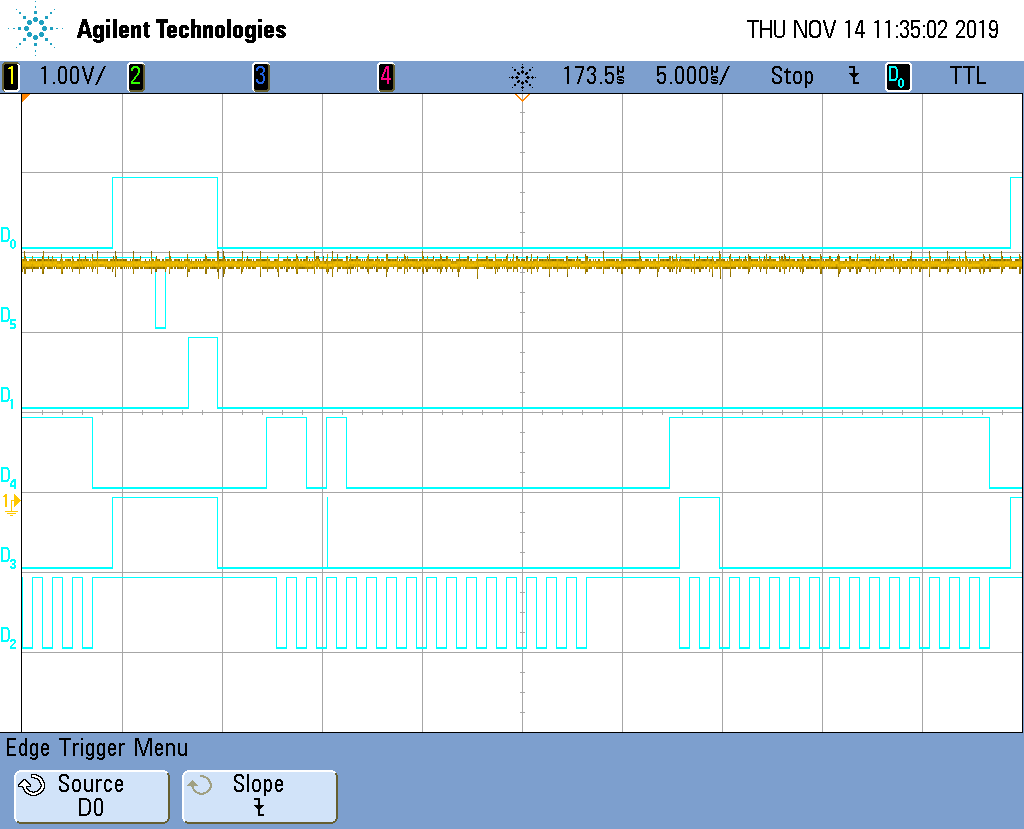
We use the manual trigger (signal CONVST, transition HIGH-LOW-HIGH, width 1us). We respect the timing between EOC and CS.

We use the tag mode and we can read the value of tag (0 to 7) in the sequence of data read by SPI.

But the converted value is always 0.

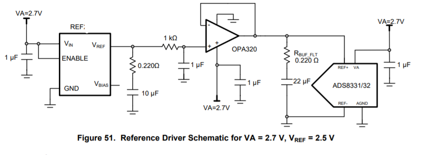
Below I insert the ADS8332 input and connection scheme.

What could be the reason why we read all the channels at 0?

Thank you very much in advance for your help.

Andrea

  • Hello Andrea,

    Welcome to the TI E2E Community.

    Based on your description, it sounds like you are correctly communicating with the ADS8332.  Assuming you are reading while the ADC is in sample mode, then you would want to follow Figure 1 in the datasheet.  If possible, please verify that all of the timing parameters are being met.

    Looking at your schematic, the REF3430 is likely not stable, and this could result in the ZERO readings that you are seeing.  Please refer to Figure 51 in the datasheet for a suggest buffer circuit.

    Some troubleshooting suggestions:

    1.  Remove all input voltages to the MUX and apply a fixed DC level directly to the input of the OPA320 ADC driver, U12.  This will help isolate any multiplexer issues with the ADC input.  Also verify the output voltage on U12 closely matches the input voltage.

    2.  Look at the REF voltage while converting.  If using a scope, you will see a voltage dip but it should quickly recover to 3V.  If using a DMM, the average value should be very close to 3V.

    3.  Verify that there is 3.3V on AVDD.

    If you can capture the SPI signals during a read frame, /CONVST, /CS, EOC, SCLK, SDO, I can check it to make sure all timing requirements are met.

    Regards,
    Keith Nicholas
    Precision ADC Applications

  • Tank you for your reply.  
    I checked the voltage on Va and Vb, both at 3.3V.

    Before changing the reference, since the circuit is not the one suggested by the datasheet, I wanted to capture some oscillograms.

    In the following pictures we have: D0=CS!; D5=CONVADC!; D1 = INT; D4 = SDI; D3 = SDO; D2 = SCLK

    In the first picture we have the entire sequence of conversions (from 0 to 7 ch). The yellow trace is the signal on pin 1 of the OPA320.

    In the second, a zoom of the connection with the signal on pin 1 at a level other than zero.


    The second 16-bit word contains the channel tag. In the first only zero, apart from a glitch captured by the logic analyzer.
    In the third figure the signal captured on the VREF pin.


    Compared to the wiring diagram posted, we added two 10uF capacitors on the reference output.

    I await your comments on the figures posted above. It is important for us to understand if it is correct that in these conditions the converted value is always 0.
    Thank you very much for your suggestions. 

    Andrea


  • Hello Andrea,

    Are you setting the ADS8332 into NAP mode?  You mentioned that you set the CFG register to 0x0F37.  Was this just a test case?

    The multiplexer is switching, as shown on the output of the OPA320 as well as the TAG bits.  I assume you are using the /INT feature on pin 10.  Please make sure the CFG is set to 0xF3F to eliminate any power-down issues.

    Also, were you able to confirm that the REF voltage is close to the expected value?

    Regards,
    Keith

  • Hello Keith,

    the problem was the NAP mode. Now it converts correctly. Thank you!

    Does he suggest changing the reference circuit or do you think it can work this way too?

    Thank you very much.

    Andrea

  • Hi Andrea,

    I am glad it is working correctly for you now.

    Without the reference buffer, you will not be able to get 16b performance at 500ksps.  Depending on how unsettled the reference is during conversion, you could see a large increase in noise, reducing the effective resolution of your ADC to 12b or less.  However, if you are sampling at a very low rate, you may be able to avoid using a reference buffer.

    Based on your previous waveforms, it looks like you are converting at 20ksps.  If this is your typical conversion rate, then you may get decent performance.  I would suggest increasing the output capacitance on the reference to 10uF, and then verify if noise meets your requirements.

    Regards,
    Keith