Hi,
I wish to come back on this DDC316 topic which I have posted couple of months ago.
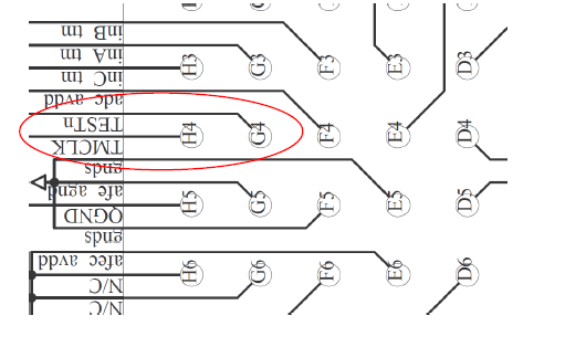
We follow the link you sent out and downlaod the sample circuit diagram.(Attached File)doc01837120200309162027.pdf
We are in the final stage of designing the PCB circuit. However, we found that some discrepancy between the datasheet and sample circuit description about the pinout of DDC316 BGA package.
Please see atatchment is the sample circuit from TI on DDC316 BGA. G4 is labelled as TSETn, and H4 is labelled as TMCLK.
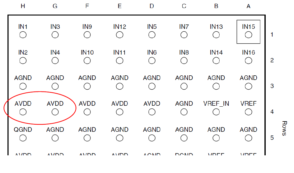
However, inside the datasheet, the pin label for G4 is AVDD, and H4 also AVDD. Can you check with TI engineer which one is correct?


