This thread has been locked.

If you have a related question, please click the "Ask a related question" button in the top right corner. The newly created question will be automatically linked to this question.

TLC5620: DAC is not generating desired output

Part Number: TLC5620

I am attempting to use the TLC5620, but I am unable to generate the desired output. I am using the following configuration:

Vdd = REFA-D = 5 V

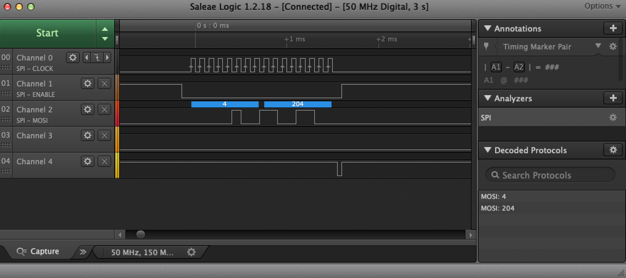
As an example: I tried to generate a 4 V output on DACB. The SSI signal (shown below) is as expected. The connections in the figure are:

  • Channel 0 [Clock] -> CLK (Pin 7)
  • Channel 1 [Enable] -> LDAC (Pin 13)
  • Channel 2 [MOSI] -> DATA (Pin 6)
  • Channel 3 -> unused
  • Channel 4 -> LOAD (Pin 8). Channel 3 is unused.

The first byte sets the Address as DACB with RNG = 0, and the data byte should set the output at 4 V (5 * 204/256 = 3.984 V. However, the output this generates is 2.059 V on DACA.

What am I doing incorrectly?

  • Hi Nelson,

    Thanks for writing to us. I am assuming your SPI communication is fine with respect to the plots you attached here. 

    1. LDAC can you make it low completely? This is just for a check. 

    2. Are you able to load another code and see change in output voltage even if its wrong value?

    Can you please share your schematics? whats the load on the DAC output?

    Please probe supply voltage and reference voltage to see there is no drop in voltage.

    As such your communication looks fine to me. These are just debug steps to proceed further.

    Regards,

    AK

  • 1. Yes, connecting LDAC to GND results in the same behavior.

    2. Other code does change the output. For example, writing 3 V to DACC results in 0.249 V on DACA (0 V on all other DACs). Writing 4 V to DACD results in 2.059 V on DACC (0 V on all other DACs).

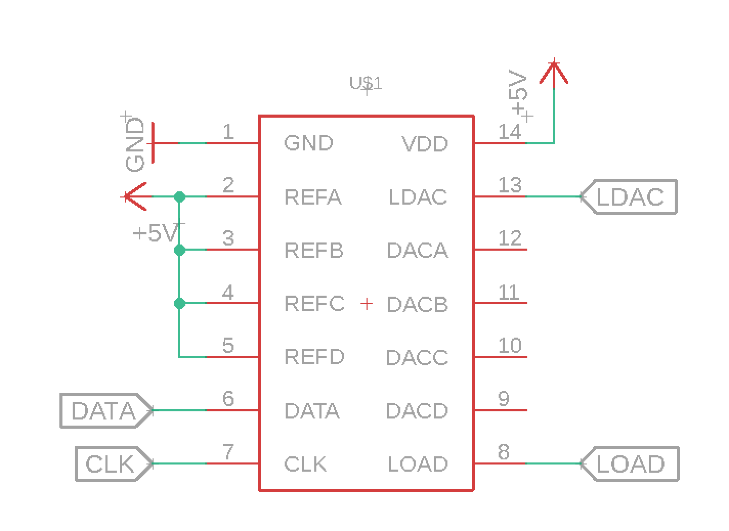
    3. The schematic is shown below. Pin 13 was connected to GND for test 1 above. I have tried both leaving the DAC output floating and connecting a 1.7k resistor to GND.

    4. The supply voltage does not drop when the output is generated. However, it is not well regulated, and is at 5.129 V.

    Thank you for your assistance. Do you have any suggestions based on these results?

  • Hi Nelson,

    Your reference has to be VDD-1.5V, in your case VDD is 5V, so Reference cannot be at 5V, max allowed is 3.5V.

    Please have a look at the datasheet and connect appropriate reference voltage.

    Regards,

    AK

  • Thank you, I had missed that in the datasheet.

    I now have all REF pins connected to 3.3 V. The code has been adjusted accordingly, and the RNG bit is now 1 to achieve a similar voltage range. However, the output is still not as expected. I have done more substantial testing to try to identify trends. It does not appear to be something as simple as the frame being shifted left or right. Below are some of my observations:

    • Writing to DACA (bits 9-10 = 00), DACB (bits 9-10 = 01), and DACD (bits 9-10 = 11) result in output on the correct DAC pins. Writing to DACC (bits 9-10 = 10) results in output on DACA instead.
    • I performed a voltage sweep to try to generate target voltages in intervals of 1 V. 0 V (0x00) gave an output of ~0V, 1 V (0x26) gave 0.064V, 2 V (0x4D) gave 0.115V, 3 V (0x74) gave 1.243V, 4 V (0x9B) gave 0.469V, 5 V (0xC1) gave 3.304V.
    • I performed a voltage sweep of 8 values 0x01, 0x02, 0x04, 0x08, 0x10, 0x20, 0x40, and 0x80. Any output that includes only a single 1 all result in an output equal to GND.

    I have confirmed that the SPI communication is behaving as expected for each test. I am not sure what is not working correctly. Do you have any further suggestions?

  • Hi Nelson,

    Ref  = 3.3V and VDD = 5V, you cant expect the device to give output range of 2*Vref. So in your case RNG bit has to be '0'. RNG can be set to '1', only when your reference is less than or equal to 2.5V and VDD  = 5V.

    with your configuration right now, when you send FF you should expect 3.3V only, not 5V , but its an invalid configuration of the device anyway, So I cant comment on that as well, device may misbehave.

    So please change reference or RNG bit and try.

    Coming back to configuration, it should work as expected. Ideally writing 10 should results in DAC C update. 

    Can you try with a new device with all the suggestions above?

    I cant test this out since because of COVID-19 we are all working from home and lab access is not there. I can only give suggestions based on experience and datasheet info for time being.

    Regards,

    AK

  • I adjusted the output to be 0-3.3 V with RNG = 0, and the device is still exhibiting the same behavior. I also tried a fresh IC in case there was something wrong with it, but that didn't fix anything.

    I understand that you cannot test things. I will try some other DAC ICs in the mean time. Thank you for your help.

  • Hi Nelson,

    Output update is the issue here now or DAC C update by writing to 10?

    Also how are you feeding reference to Pin? Is there capacitor connected to Ref  pin? Min 470pF should be connected to Ref pin and 1uF and 0.1uF should be there for supply pins.

    Please have these in schematics as I didn't see these in the diagram you shared

    Regards,

    AK

  • Hi Nelson,

    Do you need any more help here? I am assuming your issue got resolved.

    Regards,

    AK