Hi,
I'm trying to use this DAC as shown in the circuit below

When I measure the tespoints 8.9,10 and 11 I see -3V and output of the DAC is 0V.
SPI signals seem fine. This is what I see
SPICLK and SPIMO

SPICLK and SYNC

Hi,
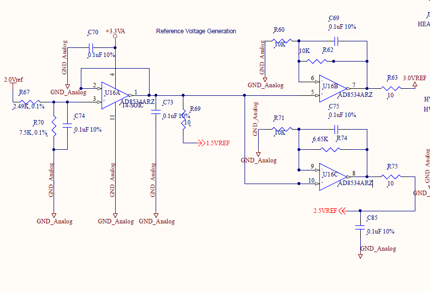
I'm trying to use this DAC as shown in the circuit below
When I measure the tespoints 8.9,10 and 11 I see -3V and output of the DAC is 0V.
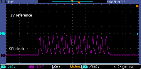
SPI signals seem fine. This is what I see
SPICLK and SPIMO
SPICLK and SYNC