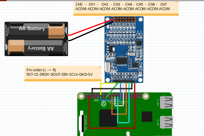
This thread has been locked.

If you have a related question, please click the "Ask a related question" button in the top right corner. The newly created question will be automatically linked to this question.

ADS1256: Getting different readings when using differential mode vs common mode on ADS1256

Part Number: ADS1256

Hi,

I have a ADS1256 hooked up to a Raspberry Pi 4 and I'm trying to read DC voltages on the analog pins of the ADS1256. The DC voltage I'm currently reading is 2.54 V from a DC power supply. The power supply itself has a common ground; therefore, it's feeding common ground signal to the ADS1256. When using the common mode, I connected the red (positive) wire to channel 0 and the black (ground) to the ACOM pin adjacent to channel 0. I then collected 5 min worth of data and the values I was getting average to 2.55 V which is very close to the original 2.54 V. I also noticed a lot of noises on the remaining analog pins. Even though they weren't connected, they were picking voltages close to 1.25 V. For my project, I need at least 3 channels and at most 4 channels.

I then tried the differential mode. I connected the red wire to channel 0 and the black wire to channel 1. I also collected the data for 5 min and this time the value averaged to 2.41 V which is way off of the original 2.54 V. For the differential mode, the other channels read a value close to 0.004 V which is quite consistent giving that the other channels aren't connected to anything. The ultimate goal is read the channels with the lowest noise possible. I was told that differential mode should perform relatively better than the common mode in terms of noise reduction but I don't know why I'm getting contradictory data. My first assumption was that since the signal being fed isn't differential per se, the analog pins have trouble reading the values. 

My current settings for the ADS is 1000SPS , GAIN = 1, clock division = 256 and the software I'm using is in C.

  • Hi user,

    Do you have a schematic to share that shows how you are connecting the inputs and supply voltages to the ADS1256? Can you also share your register settings? These might help diagnose the issue.

    In general, differential inputs are recommended for common-mode noise rejection. But AINCOM is effectively just another analog input - it could just as easily be referred to as AIN8. You can see it has the same input structure as shown in Figure 6. If you are measuring between some voltage and GND, that is a single-ended measurement, regardless of the pins you choose. So there is no meaningful difference between the two measurements you described, at least from the ADC's perspective.

    Let me know.

    -Bryan

  • Hi Brian,

    This is the setting I have. The first schematic is for the common mode reading and the second one is for the differential reading.

    Here are my register settings:

    /* gain channel  */
    typedef enum
    {
    	ADS1256_GAIN_1			= (0),	/* GAIN   1 */
    	ADS1256_GAIN_2			= (1),	/*GAIN   2 */
    	ADS1256_GAIN_4			= (2),	/*GAIN   4 */
    	ADS1256_GAIN_8			= (3),	/*GAIN   8 */
    	ADS1256_GAIN_16			= (4),	/* GAIN  16 */
    	ADS1256_GAIN_32			= (5),	/*GAIN    32 */
    	ADS1256_GAIN_64			= (6),	/*GAIN    64 */
    } ADS1256_GAIN_E;
    
    /* Sampling speed choice*/
    /* 
    	0xF0  11110000 = 30,000SPS (default)
    	0xE0  11100000 = 15,000SPS
    	0xD0  11010000 = 7,500SPS
    	0xC0  11000000 = 3,750SPS
    	0xB0  10110000 = 2,000SPS
    	0xA1  10100001 = 1,000SPS
    	0xA2  10010010 = 500SPS
    	0x82  10000010 = 100SPS
    	0x72  01110010 = 60SPS
    	0x63  01100011 = 50SPS
    	0x53  01010011 = 30SPS
    	0x43  01000011 = 25SPS
    	0x33  00110011 = 15SPS
    	0x23  00100011 = 10SPS
    	0x13  00010011 = 5SPS
    	0x03  00000011 = 2.5SPS
    */
    
    typedef enum
    {
    	ADS1256_30000SPS = 0,
    	ADS1256_15000SPS,
    	ADS1256_7500SPS,
    	ADS1256_3750SPS,
    	ADS1256_2000SPS,
    	ADS1256_1000SPS,
    	ADS1256_500SPS,
    	ADS1256_100SPS,
    	ADS1256_60SPS,
    	ADS1256_50SPS,
    	ADS1256_30SPS,
    	ADS1256_25SPS,
    	ADS1256_15SPS,
    	ADS1256_10SPS,
    	ADS1256_5SPS,
    	ADS1256_2d5SPS,
    	ADS1256_DRATE_MAX
    } ADS1256_DRATE;
    void ADS1256_CfgADC(ADS1256_GAIN_E _gain, ADS1256_DRATE _drate)
    {
    	ADS1256_WaitDRDY();
    	//g_tADS1256.Gain = _gain;
    	//g_tADS1256.DataRate = _drate;
    
    
    	uint8_t buf[4];		/* Storage ads1256 register configuration parameters */
    
    		/*Status register define
    			Bits 7-4 ID3, ID2, ID1, ID0  Factory Programmed Identification Bits (Read Only)
    			Bit 3 ORDER: Data Output Bit Order
    				0 = Most Significant Bit First (default)
    				1 = Least Significant Bit First
    			Input data  is always shifted in most significant byte and bit first. Output data is always shifted out most significant
    			byte first. The ORDER bit only controls the bit order of the output data within the byte.
    			Bit 2 ACAL : Auto-Calibration
    				0 = Auto-Calibration Disabled (default)
    				1 = Auto-Calibration Enabled
    			When Auto-Calibration is enabled, self-calibration begins at the completion of the WREG command that changes
    			the PGA (bits 0-2 of ADCON register), DR (bits 7-0 in the DRATE register) or BUFEN (bit 1 in the STATUS register)
    			values.
    			Bit 1 BUFEN: Analog Input Buffer Enable
    				0 = Buffer Disabled (default)
    				1 = Buffer Enabled
    			Bit 0 DRDY :  Data Ready (Read Only)
    				This bit duplicates the state of the DRDY pin.
    			ACAL=1  enable  calibration
    		*/
    	//buf[0] = (0 << 3) | (1 << 2) | (1 << 1);// buffer ON, auto-cal ON
             buf[0] = (0 << 3) | (1 << 2) | (0 << 1);  // buffer OFF, auto-cal ON
    
            //ADS1256_WriteReg(REG_STATUS, (0 << 3) | (1 << 2) | (1 << 1));
    
    	buf[1] = 0x08;	
    
    		/*	ADCON: A/D Control Register (Address 02h)
    			Bit 7 Reserved, always 0 (Read Only)
    			Bits 6-5 CLK1, CLK0 : D0/CLKOUT Clock Out Rate Setting
    				00 = Clock Out OFF
    				01 = Clock Out Frequency = fCLKIN (default)
    				10 = Clock Out Frequency = fCLKIN/2
    				11 = Clock Out Frequency = fCLKIN/4
    				When not using CLKOUT, it is recommended that it be turned off. These bits can only be reset using the RESET pin.
    			Bits 4-3 SDCS1, SCDS0: Sensor Detect Current Sources
    				00 = Sensor Detect OFF (default)
    				01 = Sensor Detect Current = 0.5 uA
    				10 = Sensor Detect Current = 2  uA
    				11 = Sensor Detect Current = 10 uA
    				The Sensor Detect Current Sources can be activated to verify  the integrity of an external sensor supplying a signal to the
    				ADS1255/6. A shorted sensor produces a very small signal while an open-circuit sensor produces a very large signal.
    			Bits 2-0 PGA2, PGA1, PGA0: Programmable Gain Amplifier Setting
    				000 = 1 (default)
    				001 = 2
    				010 = 4
    				011 = 8
    				100 = 16
    				101 = 32
    				110 = 64
    				111 = 64
    		*/
    	buf[2] = (0 << 5) | (0 << 3) | (_gain << 0);
    		// ADS1256_WriteReg(REG_ADCON, (0 << 5) | (0 << 2) | (GAIN_1 << 1));	/* choose 1: gain 1 ;input 5V */
    
    	buf[3] = ADS1256_DRATE_E[_drate];	// DRATE_10SPS;	
    
    		CS_0();	// SPI CS = 0   (CS active low. Doc claims no setup time needed after this)
    
            //ADS1256_WaitDRDY();
    
    	ADS1256_Send8Bit(CMD_WREG | 0);	/* Write command register, send the register address */
    	bsp_DelayUS(10);
    	ADS1256_Send8Bit(0x03);			/* Register number 4,Initialize the number   */
            bsp_DelayUS(10);
    	ADS1256_Send8Bit(buf[0]);	/* Set the status register */
    	bsp_DelayUS(10);
    	ADS1256_Send8Bit(buf[1]);	/* Set the input channel parameters */
    	bsp_DelayUS(10);
    	ADS1256_Send8Bit(buf[2]);	/* Set the ADCON control register,gain */
    	bsp_DelayUS(10);
    	ADS1256_Send8Bit(buf[3]);	/* Set the output rate */
    	bsp_DelayUS(10);
    
    	CS_1();	/* SPI  CS = 1 */
    bsp_DelayUS(10);
    
            // printf("drate: %d  Buf3 = %d, %02x\n",_drate,buf[3], buf[3]);
    
    	//bsp_DelayMS(1);
    }


    This is how I'm currently reading the data:

    static int32_t ADS1256_ReadData(void)
    {
    	
    	 uint32_t read = 0;
             static uint8_t buf[3];
    
    	CS_0();	/* SPI   CS = 0 */
    	
    	ADS1256_WaitDRDY();  // wait for ADC result to be ready
    	ADS1256_Send8Bit(CMD_RDATA);	/* Write the register number */
    	//ADS1256_WriteCmd(CMD_RDATA); // start continuous reading mode
    	
       // ADS1256_WaitDRDY();  // wait for ADC result to be ready
        	
            ADS1256_DelayDATA();    /*delay time  */
    	   //ADS1256_WriteCmd(CMD_RDATAC); // start continuous reading mode
               //bsp_DelayMS(20);


    	    //ADS1256_WriteCmd(CMD_RDATAC); // start continuous reading mode
              // bsp_DelayMS(2);


        // read the 3 byte ADC value
        buf[0] = ADS1256_Recive8Bit();
        //bsp_DelayMS(5);
        buf[1] = ADS1256_Recive8Bit();
        //bsp_DelayMS(5);
        buf[2] = ADS1256_Recive8Bit();
        bsp_DelayMS(2);
    
        // assemble 3 bytes into one 32 bit word
        read = ((uint32_t)buf[0] << 16) & 0x00FF0000;
        read |= ((uint32_t)buf[1] << 8);
        read |= buf[2];
    
        CS_1();	/* SPI CS = 1 */
    
    	/* Extend a signed number*/
        if (read & 0x800000)
        {
    	    read |= 0xFF000000;
        }
        
        //printf("read : %ld \n",read);
        //exit(0);
    
        return (int32_t)read;
    } // end ADS1256_ReadData()


    Thanks,


  • Hi user,

    Do you have an actual schematic? That image is hard to read, and it's not clear what the voltage levels are or how they are derived. For example, what is the VREF voltage you are using, and how is it generated? What about the clocking scheme? This looks like it might be a pre-built board that you are using, so a user's guide or something similar would be helpful.

    Can you read back the register settings used to take both sets of measurements and provide those to me? You mentioned you used 1000SPS in your original post, but your code shows 10SPS, so I am not sure which settings are actually valid for the issue you are seeing.

    Are you really using 2 AA batteries as the input? You mentioned a DC power supply, so I imagined a bench top device. I just want to make sure I understand your actual setup.

    How are you reading the voltage levels on the adjacent channels? You said there was 1.25V on adjacent inputs when you tied the DC GND to AINCOM - did you measure this with a DMM, or with the ADC?

    -Bryan