


Other Parts Discussed in Thread: ADC31JB68EVM, DAC38J84, ADS54J69EVM
Dear TI Supporters,
I am testing with DAC38J84EVM + TSW14J10 + ZCU106(Xilinx Ev board with ZCU7EV).
I have modified "TI_HSDC_Pro_Reference_design_V2.8" as attached zip file, for Vivado 2019.2 and ZCU106 board.
I have modified and added 3 board settings in scripts as below.
- ZCU106_1P: with JESD204B 1 pair(2 lanes) link, for ADC31JB68EVM. It was successful.
- ZCU106_2P: with JESD204B 2 pairs(4 lanes) link, for DAC38J84EVM. SYNC is low. Sending data stuck at “WriteDrpReg()” function.
- ZCU106_4P: with JESD204B 4 pairs(8 lanes) link, for DAC38J84EVM. SYNC is low.
My target setting is ZCU106_2P.
ZCU106_4P is just for test.
### With both settings, SYNC is low.
I have checked it with D3 LED, that is connected sync_led output from FPGA.
And, I also checked it with ALARM test point and dtest setting(0100, SYNC, config27)
I have done below modification from TSW14J10EVM user guide.
Because ZCU106 also have no connection in FMC connector for tx_syncp/tx_syncn, as ZC706.
The ZC706 development platform does not have traces routed on FMC connector pins F10 and F11,
which are normally used for the JESD204B DAC SYNC differential signals. To accommodate for this, the
TSW14J10EVM has options to move the SYNC signals to FMC pins H19 and H20 by making the following
resistor changes:
1. Remove R143, R145.
2. Install 0-Ω resistors for R142, R144, R146, and R149.
These resistors are all located on the bottom side of the TSW14J10EVM near the FMC connector.
### ZCU106_2P setting stuck at “WriteDrpReg()” function when send data.
ZCU106_4P setting doesn’t stuck at WriteDrpReg function when send data.
I have attached debug messages from microblaze firmware for both settings.
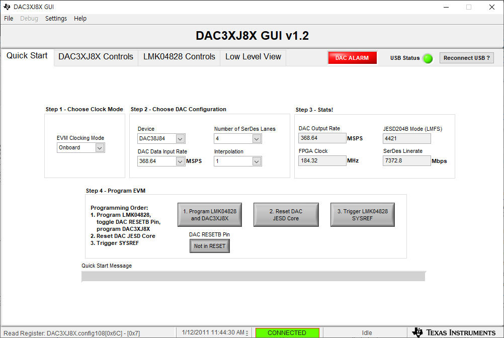
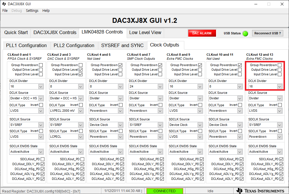
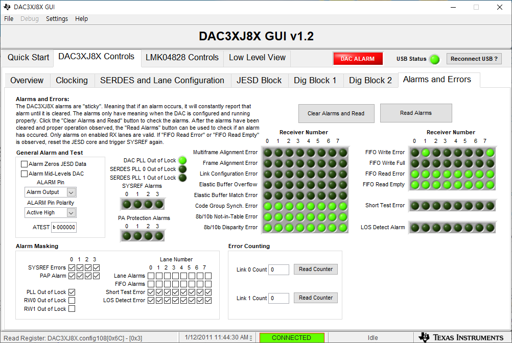
Belowes are Quick Start, LM04828 Clock Outputs setting, and Alarms after sending data from HSDC pro, for ZCU106_2P setting.

Belowes are Quick Start, LM04828 Clock Outputs setting, and Alarms after sending data from HSDC pro, for ZCU106_4P.

Clock Outpus Setting is same with ZCU106_2P.

I have also attached debug messages from microblaze firmware.
I have analyzed those messages, but cannot find cause of the problems.
Please, check my modifications and GUI settings.
****************************************
* Starting the TSW microblaze software *
* Version 2.8.000                      *
****************************************
2.8 2016.1 build
##############################################

Platform ID = 0x68
JESD Status= 0xFFFFF8F8
Writing to JESD GPIO1 0x00000120
Writing to JESD GPIO1 0x00000020
JESD Status= 0xFFFEF0F0


......Initialisation Complete.....

Jesd204Status   = 0x88
DataBlockStatus = 0x22
PHY PLL Status  = 0x05
Processing a command from the Queue. Received data is:
scmd=0x0 bank=0x000 addr=0x00000040 data=0x00000001
Write to control and status bank 0x00000040 0x00000001
ProcessCtrlCmd addr=0x00000040 data=0x00000001
Write JESD Control Register 0x00000001
Writing to JESD GPIO1 0x00000120
Processing a command from the Queue. Received data is:
scmd=0x0 bank=0x000 addr=0x00000044 data=0x00000040
Write to control and status bank 0x00000044 0x00000040
ProcessCtrlCmd addr=0x00000044 data=0x00000040
Write JESD Line Rate Config Register
Writing to JESD GPIO1 0x00000120
Processing a command from the Queue. Received data is:
scmd=0x0 bank=0x000 addr=0x00000048 data=0x00000002
Write to control and status bank 0x00000048 0x00000002
ProcessCtrlCmd addr=0x00000048 data=0x00000002
Write JESD Config Register 1 0x00000002
Writing to JESD GPIO1 0x00000120
Processing a command from the Queue. Received data is:
scmd=0x0 bank=0x000 addr=0x0000004C data=0x00080000
Write to control and status bank 0x0000004C 0x00080000
ProcessCtrlCmd addr=0x0000004C data=0x00080000
Write JESD Config Register 2  0x00080000
Processing a command from the Queue. Received data is:
scmd=0x0 bank=0x002 addr=0x00000008 data=0x00000001
Write to JESD204 TX bank 0x00000008 0x00000001
Processing a command from the Queue. Received data is:
scmd=0x0 bank=0x002 addr=0x0000000C data=0x00000000
Write to JESD204 TX bank 0x0000000C 0x00000000
Processing a command from the Queue. Received data is:
scmd=0x0 bank=0x002 addr=0x00000010 data=0x00000000
Write to JESD204 TX bank 0x00000010 0x00000000
Processing a command from the Queue. Received data is:
scmd=0x0 bank=0x002 addr=0x00000014 data=0x00000003
Write to JESD204 TX bank 0x00000014 0x00000003
Processing a command from the Queue. Received data is:
scmd=0x0 bank=0x002 addr=0x00000018 data=0x00000000
Write to JESD204 TX bank 0x00000018 0x00000000
Processing a command from the Queue. Received data is:
scmd=0x0 bank=0x002 addr=0x00000020 data=0x00000001
Write to JESD204 TX bank 0x00000020 0x00000001
Processing a command from the Queue. Received data is:
scmd=0x0 bank=0x002 addr=0x00000024 data=0x00000009
Write to JESD204 TX bank 0x00000024 0x00000009
Processing a command from the Queue. Received data is:
scmd=0x0 bank=0x002 addr=0x00000028 data=0x0000000F
Write to JESD204 TX bank 0x00000028 0x0000000F
Processing a command from the Queue. Received data is:
scmd=0x0 bank=0x002 addr=0x0000002C data=0x00000001
Write to JESD204 TX bank 0x0000002C 0x00000001
Processing a command from the Queue. Received data is:
scmd=0x0 bank=0x002 addr=0x00000034 data=0x00000000
Write to JESD204 TX bank 0x00000034 0x00000000
Processing a command from the Queue. Received data is:
scmd=0x0 bank=0x002 addr=0x0000080C data=0x00000ABC
Write to JESD204 TX bank 0x0000080C 0x00000ABC
Processing a command from the Queue. Received data is:
scmd=0x0 bank=0x002 addr=0x00000818 data=0x00001234
Write to JESD204 TX bank 0x00000818 0x00001234
Processing a command from the Queue. Received data is:
scmd=0x0 bank=0x002 addr=0x00000004 data=0x00000001
Write to JESD204 TX bank 0x00000004 0x00000001
Processing a command from the Queue. Received data is:
scmd=0x0 bank=0x000 addr=0x00000040 data=0x00000003
Write to control and status bank 0x00000040 0x00000003
ProcessCtrlCmd addr=0x00000040 data=0x00000003
Write JESD Control Register 0x00000003
Reconfigure Gt's for freq band=4
ConfigureChannelDrp setting=4
XCVR read  0x0000005E, 0x00000000
write 0x00000002
XCVR read  0x0000005E, 0x00000002
write 0x00000082
XCVR read  0x0000005E, 0x00000082
write 0x00001082
XCVR read  0x00000088, 0x000002AA
write 0x000002A8
XCVR read  0x00000088, 0x000002A8
write 0x00000288
XCVR read  0x000000A8, 0x0000B46B
write 0x00000020
XCVR read  0x000000A9, 0x0000280A
write 0x00001040
XCVR read  0x000000AA, 0x000024A4
write 0x000023FF
XCVR read  0x000000AB, 0x0000280A
write 0x00000000
XCVR read  0x000000AC, 0x00000000
write 0x0000000B
ConfigureCommonDrp setting=4
QPLL read  0x00000036, 0x00000000
write 0x00000030
QPLL read  0x00000033, 0x00000000
write 0x00008000
QPLL read  0x00000032, 0x00000000
write 0x00000181
QPLL read  0x00000033, 0x00008000
write 0x00008068
QPLL read  0x00000036, 0x00008000
w
****************************************
* Starting the TSW microblaze software *
* Version 2.8.000                      *
****************************************
2.8 2016.1 build
##############################################

Platform ID = 0x78
JESD Status= 0xFFFFF8F8
Writing to JESD GPIO1 0x00000120
Writing to JESD GPIO1 0x00000020
JESD Status= 0xFFFEF0F0


......Initialisation Complete.....

Jesd204Status   = 0x88
DataBlockStatus = 0x22
PHY PLL Status  = 0x05
Processing a command from the Queue. Received data is:
scmd=0x0 bank=0x000 addr=0x00000040 data=0x00000001
Write to control and status bank 0x00000040 0x00000001
ProcessCtrlCmd addr=0x00000040 data=0x00000001
Write JESD Control Register 0x00000001
Writing to JESD GPIO1 0x00000120
Processing a command from the Queue. Received data is:
scmd=0x0 bank=0x000 addr=0x00000044 data=0x00000030
Write to control and status bank 0x00000044 0x00000030
ProcessCtrlCmd addr=0x00000044 data=0x00000030
Write JESD Line Rate Config Register
Writing to JESD GPIO1 0x00000120
Processing a command from the Queue. Received data is:
scmd=0x0 bank=0x000 addr=0x00000048 data=0x00000002
Write to control and status bank 0x00000048 0x00000002
ProcessCtrlCmd addr=0x00000048 data=0x00000002
Write JESD Config Register 1 0x00000002
Writing to JESD GPIO1 0x00000120
Processing a command from the Queue. Received data is:
scmd=0x0 bank=0x000 addr=0x0000004C data=0x00080000
Write to control and status bank 0x0000004C 0x00080000
ProcessCtrlCmd addr=0x0000004C data=0x00080000
Write JESD Config Register 2  0x00080000
Processing a command from the Queue. Received data is:
scmd=0x0 bank=0x002 addr=0x00000008 data=0x00000001
Write to JESD204 TX bank 0x00000008 0x00000001
Processing a command from the Queue. Received data is:
scmd=0x0 bank=0x002 addr=0x0000000C data=0x00000000
Write to JESD204 TX bank 0x0000000C 0x00000000
Processing a command from the Queue. Received data is:
scmd=0x0 bank=0x002 addr=0x00000010 data=0x00000000
Write to JESD204 TX bank 0x00000010 0x00000000
Processing a command from the Queue. Received data is:
scmd=0x0 bank=0x002 addr=0x00000014 data=0x00000003
Write to JESD204 TX bank 0x00000014 0x00000003
Processing a command from the Queue. Received data is:
scmd=0x0 bank=0x002 addr=0x00000018 data=0x00000000
Write to JESD204 TX bank 0x00000018 0x00000000
Processing a command from the Queue. Received data is:
scmd=0x0 bank=0x002 addr=0x00000020 data=0x00000000
Write to JESD204 TX bank 0x00000020 0x00000000
Processing a command from the Queue. Received data is:
scmd=0x0 bank=0x002 addr=0x00000024 data=0x00000013
Write to JESD204 TX bank 0x00000024 0x00000013
Processing a command from the Queue. Received data is:
scmd=0x0 bank=0x002 addr=0x00000028 data=0x000000FF
Write to JESD204 TX bank 0x00000028 0x000000FF
Processing a command from the Queue. Received data is:
scmd=0x0 bank=0x002 addr=0x0000002C data=0x00000001
Write to JESD204 TX bank 0x0000002C 0x00000001
Processing a command from the Queue. Received data is:
scmd=0x0 bank=0x002 addr=0x00000034 data=0x00000000
Write to JESD204 TX bank 0x00000034 0x00000000
Processing a command from the Queue. Received data is:
scmd=0x0 bank=0x002 addr=0x0000080C data=0x00000ABC
Write to JESD204 TX bank 0x0000080C 0x00000ABC
Processing a command from the Queue. Received data is:
scmd=0x0 bank=0x002 addr=0x00000818 data=0x00001234
Write to JESD204 TX bank 0x00000818 0x00001234
Processing a command from the Queue. Received data is:
scmd=0x0 bank=0x002 addr=0x00000004 data=0x00000001
Write to JESD204 TX bank 0x00000004 0x00000001
Processing a command from the Queue. Received data is:
scmd=0x0 bank=0x000 addr=0x00000040 data=0x00000003
Write to control and status bank 0x00000040 0x00000003
ProcessCtrlCmd addr=0x00000040 data=0x00000003
Write JESD Control Register 0x00000003
Reconfigure Gt's for freq band=3
ConfigureChannelDrp setting=3
XCVR read  0x0000005E, 0x00000000
write 0x00000002
XCVR read  0x0000005E, 0x00000002
write 0x00000082
XCVR read  0x0000005E, 0x00000082
write 0x00001082
XCVR read  0x00000088, 0x000002AA
write 0x000002A8
XCVR read  0x00000088, 0x000002A8
write 0x00000288
XCVR read  0x000000A8, 0x0000B46B
write 0x00000020
XCVR read  0x000000A9, 0x0000280A
write 0x00001040
XCVR read  0x000000AA, 0x000024A4
write 0x000023FF
XCVR read  0x000000AB, 0x0000280A
write 0x00000000
XCVR read  0x000000AC, 0x00000000
write 0x0000000B
ConfigureCommonDrp setting=3
QPLL read  0x00000036, 0x00000000
write 0x00000030
QPLL read  0x00000033, 0x00000000
write 0x00008000
QPLL read  0x00000032, 0x00000000
write 0x000001C1
QPLL read  0x00000033, 0x00008000
write 0x00008068
QPLL read  0x00000036, 0x00000000
write 0x00000030
QPLL read  0x00000033, 0x00000000
write 0x00008000
QPLL read  0x00000032, 0x00000000
write 0x000001C1
QPLL read  0x00000033, 0x00008000
write 0x00008068
Writing to JESD GPIO1 0x00000120
Processing a command from the Queue. Received data is:
scmd=0x0 bank=0x000 addr=0x00000040 data=0x00000000
Write to control and status bank 0x00000040 0x00000000
ProcessCtrlCmd addr=0x00000040 data=0x00000000
Write JESD Control Register 0x00000000
Writing to JESD GPIO1 0x00000020
Processing a command from the Queue. Received data is:
scmd=0x0 bank=0x000 addr=0x00000024 data=0x000000FF
Write to control and status bank 0x00000024 0x000000FF
ProcessCtrlCmd addr=0x00000024 data=0x000000FF
Write Data Block TX CNFG GPIO 0x00FF
Processing a command from the Queue. Received data is:
scmd=0x0 bank=0x000 addr=0x00000020 data=0x00000002
Write to control and status bank 0x00000020 0x00000002
ProcessCtrlCmd addr=0x00000020 data=0x00000002
Write Data Block TX CTRL GPIO 0x0002
Processing a command from the Queue. Received data is:
scmd=0x0 bank=0x000 addr=0x00000020 data=0x00000000
Write to control and status bank 0x00000020 0x00000000
ProcessCtrlCmd addr=0x00000020 data=0x00000000
Write Data Block TX CTRL GPIO 0x0000
Processing a command from the Queue. Received data is:
scmd=0x0 bank=0x000 addr=0x00000020 data=0x00000004
Write to control and status bank 0x00000020 0x00000004
ProcessCtrlCmd addr=0x00000020 data=0x00000004
Write Data Block TX CTRL GPIO 0x0004
Processing a command from the Queue. Received data is:
scmd=0x0 bank=0x000 addr=0x00000008 data=0x00000000
Write to control and status bank 0x00000008 0x00000000
ProcessCtrlCmd addr=0x00000008 data=0x00000000
Processing a command from the Queue. Received data is:
scmd=0x0 bank=0x000 addr=0x00000020 data=0x00000008
Write to control and status bank 0x00000020 0x00000008
ProcessCtrlCmd addr=0x00000020 data=0x00000008
Write Data Block TX CTRL GPIO 0x0008
Jesd204Status   = 0x00
DataBlockStatus = 0x22
PHY PLL Status  = 0x1D
