This thread has been locked.

If you have a related question, please click the "Ask a related question" button in the top right corner. The newly created question will be automatically linked to this question.

ADC device selection

Other Parts Discussed in Thread: ADS54J69, ADS54J60, ADC16DX370, ADS42LB69, ADC3241, THS1206, ADS8555, ADS8342, MSP430F449, TM4C123FH6PM

Hello.

Please advise ADC device selection.

ADC resolution should be 16bit.

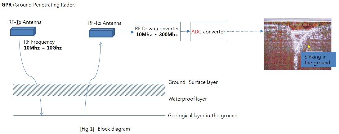
I want to convert 10 Mhz ~ 300Mhz analog frequency to ADC.

Please help by selecting ADC device.

Best Regards,
Jame, Shin

  • Jame, 

    Please specify the part number of the device you are using. 

    Yusuf

  • Hello Yusuf,

    I am not sure which part number to choose for the design I want.

    With MCU control, the ADC conversion value is first saved as a text file.

    Then, the text file is read from the PC program and the result value is displayed in graph form.

    The spec I think is below.

    -----------------------------------------------------------------

    ADC conversion time : (min) 1us       (max) 0.1us

    ADC Conversion rate : (min) 1Msps   (max) 10Msps

    ADC resolution bit   : (min) 12bit     (max) 16bit.

    ADC input channels : (min) 2 Ch     (max) 4Ch

    ADC Input Frequency : 10Mhz ~ 300 Mhz

    ADC input type : single-Ended

    MCU Interface : SPI

    -----------------------------------------------------------------

    There is a difficult part in selecting an ADC device from Ti for search.

    Q1> Which of the Precision Vs Highspeed ADC is suitable?

    Q2> I don't know what kind of architecture to choose.

            i.e) SAR, Delta-Sigma, Pipeline….,

    Q3> Please help me choose the ADC device suitable for my application.

    Best Regards,
    Jame, Shin

  • Shin:

    You will want a high speed ADC capable of supporting your analog input signal frequency.  There are many options and trade-offs with respect to performance, cost, and power consumption.  There are also different options depending on the digital interface requirements.  Based on your information above I will give you a few starting points to investigate for 16-bit resolution devices.

    JESD204B Interface

    • ADS54J69 - 16b, 500MSPS,1200MHz BW
    • ADS54J60 - 16b, 1000MSPS, 1200MHz BW
    • ADC16DX370 - 16b, 370MSPS, 800 MHz BW

    LVDS Interface

    • ADS42LB69 - 16b, 250MSPS, 900 MHz BW

    --RJH

  • Hello RJH,

    Thank you for the reply.

    From the starting point of 16bit ADC device selection, I am moving forward.

    I previously only used the ADC built into the Ti 32bit MCU, but I have a lot of trouble selecting a separate ADC device.

    Q1> How do I interface between  ADC device(JEDS204B Vs LVDS Parallel)  and  MCU?

    Q2> I would like to create a text file of the results of the ADC acquisition data with the thoughts I prepared for designing the GPR equipment.

            The reason is to make development design easy.

            Advise your thoughts and ideas.

    Q3> I am not free of cost on the ADC device you suggested.

           Reduce development specs by one step in cost.

           (Modify Spec)

            ---------------------------------------------------------------------

            ADC Input Frequency : 10 Mhz ~ 100 Mhz

            ADC input channels l : Up to 4Ch(min) ~  8Ch(max)

            ---------------------------------------------------------------------

          Would you please tell the starting point again in selecting ADC device?

    Q4> Why can't I use it as a design application with a Precision ADC device?

    Best Regards,
    Jame, Shin

  • Shin:  Please see below.  --RJH

    Q1> How do I interface between  ADC device(JEDS204B Vs LVDS Parallel)  and  MCU?

    RJH>> Not sure I can answer this.  It depends on the capabilities of the MCU and the digital interface options.  You mentioned before you used an ADC built in to the MCU.  My guess is that ADC must have been a lower sampling rate and lower performing option compared to the recommendations I provided.  Typically our high performance ADC interface to an FPGA that is capable of supporting the LVDS or JESD204B interface.  If your MCU if fixed, then you will need to work around its capabilities.

    Q2> I would like to create a text file of the results of the ADC acquisition data with the thoughts I prepared for designing the GPR equipment.

    RJH>> For prototyping or demo purposes, you can use the TI ADC with the TI capture card (used for evaluation).  The corresponding software, HSDC Pro Software, can export captured data to a file.

    Q3> I am not free of cost on the ADC device you suggested.

    RJH>>  16b and high speed together will set a price point.  You can downgrade the resolution to 14b and then some lower sampling rate options come into play.  These devices will be less expensive.

     - ADC3241   14b, 25 MSPS, 540 MHz BW, Serial LVDS interface

    Q4> Why can't I use it as a design application with a Precision ADC device?

    RJH>> You may be able to and your MCU interface may dictate a Precision ADC.  I targeted high speed converters given the nature of the application (radar signals) and the frequency up to 300 MHz.

  • Hello RJH,

    RJH_A> You may be able to and your MCU interface may dictate a Precision ADC. 

    I 'm change Precision ADC device the perspective direction.

    I searched for Ti devices(Precision ADC).

    1. ADS7863A  4Ch,  2000kSPS, 12bit ,  SPI ,          SAR
    2. THS1206    4Ch,   6000kSPS, 12bit,   Parallel,    Pipeline
    3. ADS8363    4Ch,  1000kSPS, 16bit ,  SPI ,          SAR
    4. ADS8168    8Ch , 1000kSPS, 16bit ,  SPI,           SAR

    Q1> Is it possible to convert ADC with ADC input frequency from 10Mhz to 100Mhz below?

    Q2> Please advise what to consider about the problem.

    Best Regards,
    Jame, Shin

  • Hello Jaime,

    Precision ADCs are normally not meant for undersampling applications and the analog bandwidth is usually not too far outside of the sampling frequency.  Therefore, the devices you're looking at in the last thread will not be able to undersample a 10MHz - 100MHz signal.

  • Hello Collin,

    Thank you for the reply.

    I understand what you say, but please answer the question below.

    Collin _A> Precision ADCs…normally not meant...bandwidth is usually not too far outside of the sampling frequency. 

    Q1> For THS1206 (Precision ADC), the analog input specification is specified in the differential (typ) 96Mhz, single-end (typ)54Mhz data sheet.

           What is the bandwidth of THS1206 device?

    Q2> Please suggest a device that can convert 10Mhz ~ 100Mhz signal to ADC from Precision ADCs device.

    Q3> If the question in Q2> is not answered, please suggest a device to solve.

    Best Regards,
    Jame, Shin

  • Hello Jamie,

    1.)  The THS1206 is on the high end of what's considered a Precision ADC by speed, but by application and operation it's used more like the higher-speed ADCs we'd mentioned before.  It does in fact have an analog bandwidth that's higher than the sampling rate and can be used for undersampling.

    2.)  Does the THS1206 meet your requirements? What you found in the datasheet is correct.

  • Hello Collin,

    Thank you for the reply.

    To help my understanding, please answer the question number “Qn> “In response” “An>”.

    Collin_1) The THS1206 .. . It does in fact .. analog bandwidth that's higher than the sampling rate and can ..  undersampling.

           Q1> I am worried that the precision ADC device is not wide bandwidth.

                   What is the actual THS1206 analog bandwidth range?  (single-end & differential)

    Collin_2) Does the THS1206 meet your requirements?

                   A1> No, I need ADC bit 14bit Up to 16bit and Sample rate 1Msps Up to 5Msps (Simultaneous Sampling).

    Q2> Please suggest the ADC device recommended for the application.

    Best Regards,
    Jame, Shin

  • Hi Jamie,

    We discussed the analog BW of the THS1206 in the last post and confirmed that the datasheet is correct.  I've pasted it below for reference.  The THS1206 as mentioned functions more like the high-speed ADCs Russell directed you towards earlier in the thread.

    If the device selections Russell mentioned did not work, nor do any of the THS1206 options then we may not have exactly what you need and some compromises may need to be made in the device features or performance. 

  • Hello Collin,

    Collin _said> If the device selections Russell mentioned did not work…..

                  Q1> Who is Russell? Or I don't know what it means.

                 Q2> I saw the contents of the analog input you captured in the data sheet before.

                        I don't  know BW

    Could you explain to the previous post that the question was not answered?

    Best Regards,
    Jame, Shin

  • Hi Jamie,


    Russell was the helpful TI employee working with you before me.  His handle is RJ Hopper.

    You'll find a lot of graphs in the datasheet showing performance information for input frequencies in the 200kHz - 3MHz range.  Also, Figure 21 shows the Gain vs. Frequency for a single-ended configuration which is where the single-ended bandwidth spec in the datasheet comes from.  The differential input bandwidth has a similar same shape, but the -3dB frequency is extended out to 96MHz as shown in the spec table.

  • Hello Collin,

    This is the answer you asked in the previous post.

    Collin_Q> Does the THS1206 meet your requirements?

                   -12Bit, 4Ch Simultaneous-Sampling ADC , Interface : Parallel,    Architecture : Pipeline

    Jame_A> No, I need ADC bit 14bit Up to 16bit and Sample rate 1Msps Up to 5Msps (Simultaneous Sampling).

    So I am looking at the ADS8555 Data Sheet on the Precision ADCs device.

                -16Bit, 6Ch Simultaneous-Sampling ADC , Interface : Parallel, SPI,   Architecture : SAR

                  Sample rate : 630 kSPS (Parallel),  With External Clock 800 kSPS (Parallel).

    Q1> Is it possible to ADC of the ADS8555 device to the analog input 10Mhz ~ 100Mhz range?

           Like the image captured in the previous post (Gain vs input frequency (Single-ended))

    Best Regards,
    Jame, Shin

  • Hi Jaime,

    The ADS8555 won't work.  The analog small signal bandwidth is <50MHz.  Unfortunately if none of Russell's products worked for your application and the ones we've already reviewed from the precision portfolio also don't work, then this is looking like a potential gap in our offerings.  There may be a product out there, but the primary application for precision ADCs is nyquist sampling, not undersampling which is why we're not as immediately aware of a device which meets these requirements.

  • Collin(Vendor's Russell),

    Q1> I am not sure what has to do with analog input frequency bandwidth( <50Mhz ) in relation to the Nyquist theory.

           Please explain clearly and in detail?

    Q2> Explain in detail what you mean by not undersampling.?

           The sampling frequency I know is below.

    Sampling frequency per second = (ADC Resolution bit + bit of charge/discharge time of ADC input capacitor) * Sample rate

    i.e) Sampling frequency Clock = ( 16bit + 4bit ) * 630KSPS(AD8555) = 12.6Mhz

    Best Regards,
    Jame, Shin

  • Jamie,

    1.)  Most precision ADCs (sampling rates < 5MSPS, SPI/Parallel interfaces) have primary applications of sampling signals within the bandwidth of their first Nyquist zone (Fs/2).  Therefore the typical maximum signal bandwidth of a 1MSPS precision ADC in most applications is 500kHz.  This is the primary application for these products and therefore nearly all of the datasheet specifications for them are based on operation in that frequency band. 

    Some of the portfolio's higher speed devices will also specify the -3dB small signal bandwidth (e.g. the ADS8555 specs a small signal -3dB bandwidth of nearly 50MHz, the THS1206 spec'ed 96MHz).  These devices can be used for undersampling applications in addition to Nyquist sampling applications, but as you've found we don't feature a product that exactly meets the bandwidth, resolution, and simultaneous sampling needs for the upper 100MHz frequency inputs you're requesting. 

    2.) Undersampling means that you're operating the converter in system where the fundamental input frequencies are not in the first Nyquist band of the converter.  For a 630kSPS converter, the 1st Nyquist frequency band is 315kHz.  If you carefully bandpass filter higher frequency signals then you can alias then back into the 1st Nyquist zone as described by the sampling theorem so you can actually acquire aliases of the higher frequency signals without sampling at rates high enough to capture them in the 1st zone.

  • Hello Collin, & Vendor's Russell,

    To help my understanding, I drew a picture.

    Please answer each question.

    Q1>Sampling rate 630KSPS , but 1sec/1.26㎲ = 793.7 KSPS is calculated

           Why is it different?

    Q2> Explain the meaning of Acquisition time((min) 280 ns)

           1 sec / 280 ns = 3.57…

         Does this mean acquiring 3.57 data of ADC conversion completion value per second?

    (Nyquist theory )

    When sampling an analog input signal, sampling at a frequency more than 2 times of the input signal can be converted into a complete input signal.

    Q3> Please explain the meaning of the number ±4 in the data sheet.

         –3-dB small-signal bandwidth (typ)48Mhz :  

         Input range = ±4 × VREF ,

         ±4 x 3V = -12 and +12   (Input range: 12+12=48)

    Q4> You say that the 12Mhz Fs/2 you speak is Undersampling to use on the device.

           Nyquist theory 2 times the frequency, i.e. (12Mhz sampling Frequency (Fs)) x 2 = 48Mhz

           To do this, if sampling is 48Mhz, when do you use oversampling?

    Q5> Please explain the difference between the sampling clock frequencies below. ?

           Sampling Clock frequency per second = (ADC Resolution bit + bit of charge/discharge time of ADC input capacitor) * Sample rate

         1. (My thinking)         Conversion Clock frequency = ( 16bit + 4bit ) * 630KSPS   = 12.6Mhz

         2. (Data sheet Spec. )                     Internal Conversion Clock frequency (FCCLK ) = 14.7Mhz

    Q6> What are the limitations of Vendor(Ti) Precision ADC design?

           I thought down the input signal 100Mhz for ADC conversion.

         - In the block diagram of the ADS8555 device, how many times more clocks can be input to the input signal from the clock generator block?

         - Is it possible to oversample?

    Q7> How many clocks( Internal Conversion Clock : FCCLK ) are needed in 10 ns for ADC conversion?

           e.g.) 100Mhz (10ns) , 10ns/68ns = 0.147 FCCLK

    Best Regards,
    Jame, Shin

  • Hello  all  Ti ADC Engineers,

    I am waiting to answer each question(Q1 ~Q7) from the previous post.

    Best Regards,
    Jame, Shin

  • Hi Jamie,

    We've provided you all of the ADC options we have available and have explained their capabilities.  We have also confirmed that in the precision ADC devices we have the THS1206 was our closest fit.  

    Please watch the TI Precision Labs Videos on SAR ADCs for more detailed information on acquisition timing, conversion timing, and how these devices are typically operated.  Section 3 is about ADC Drive which covers the SAR ADC operation and Section 6 is all about AC parameters and provides an in-depth review on sampling theorem and aliasing.  

    https://training.ti.com/ti-precision-labs-adcs

  • Hello Collin,

    My name is not Jamie. I'm Jame.

    Thank you for the reply.

    I searched for “Design & development” of the THS1206 device's drive software, but couldn't find it.

    And I can't find the THS1206EVM software source code.

    Best Regards,
    Jame, Shin

  • Hello Jame,

    Apologies for making a mistake with your name.

    I've attached a .ZIP file with the THS1206EVM SW.  Note that it was developed back in 2003 so it will likely not directly compile in CodeComposerStudio (CCS), but the .C and .H files should give a good understanding of an example parallel interface on an MCU.

  • Hello. Collin,

    The file you attach to me is ADS8342 (adc) & MSP430 (mcu) software.

    The device I chose after review is not TH1206 software.

    The two devices have the same parallel interface but different pin functions and operation.

    And I analyzed the source code you sent, but the source code is not complete.

    (For example)

      1.The contents of the source code are different and only the THS1206.c file name is the same.

      2. 15pin CONV_CLK(CVST) of THS1206 device does not have clock generation source code.

      3. Initialization source code of TH1206 device is not shown. In Datasheet (Figure 34. THS1206 Configuration Flow)

      4. In Control Register 0 / 1, there is no source code for initial value or setting value.

      5. Since there is no parallel interface function in Mcu, it is necessary to make timing with GPIO mode for a limited time.

           However, the source code is not visible.

      6. Others , etc……,

    Please check if it is the source code to run THS1206 device.

    Best Regards,
    Jame, Shin

  • Hello Jame,

    The code we provided directly is what was shipped out to help test the THS1206EVMs when they were manufactured.  It is was based on the ADS8342 as you noted with some minor changes for the THS1206.  It was not intended to be a fully complete project and will require modifications to fit your end-system integration.  We don't have a fully public code example so what we provided is the best we have to offer right now.

  • Hello Collin,

    All right, I understand about your said.

    I ask sequential questions about THS1206 device.

    I want to answer sequentially.

    Jul 21_Q1> THS1206EVMs What kind of tests do you do in detail when manufacturing?

    Jul 21_Q2> Do you test the CONV_CLK(CVST) signal in either single conversion mode and continuous conversion mode?

    Jul 21_Q3> Do you test circular buffer (16x12bit FIFO) read and write?

    Jul 21_Q4> When selecting one analog input, do you test by selecting trigger levels 1, 4, 8 and 14?

    Best Regards,
    Jame, Shin

  • Hello. ADC Forum all engineer.

    There are single conversion mode and continuous conversion mode of THS1206 device.

    Continuous conversion mode provides external (max) 6Mhz to 15 pins of CONS_CLK(CONVST) of THS1206.

    The single conversion mode is described below in the datasheet.

    However, there is no block diagram of the internal oscillator function in the function block diagram.

    (In Datasheet THS1206)

    “The internal clock oscillator is switched off in continuous conversion mode “

    “ The conversion clock in single conversion mode is generated internally using a clock oscillator circuit. “

    Jul 27_Q5> In single conversion mode, do not supply an external clock to 15Pin(CONV_CLK(CONVST))?

                   I don't understand that it is switching from external clock to internal oscillator.

    Best Regards,
    Jame, Shin

    Ps,I am waiting for the answer from previous post Jul 21_Q1> to Q4>.

  • Hi Jame, Shin,

    Q1-Q4:  TI does not disclose production test information of our products or EVMs.  The software provided previously was provided as our best offering to help get you going, but we will not support questions on unreleased/unofficial code examples.

    You've done a great job reading through the code an identifying what functions have/haven't been implemented.  We will continue answering the questions you posed this AM in the next post.

  • Hello Jame,

    Regarding your question 5, yes, in single conversion mode, you do not apply an external clock to the 15Pin(CONV_CLK(CONVST).  This mode of operation is useful if you do not need the maximum data rate of the device.  For example, in continuous conversion mode, the sampling rate can range from 100ksps up to 6Msps for a single channel.  In single conversion mode, the sampling rate can range from 0 up to 3Msps for a single channel.

    You select between continuous and single conversion modes by writing to Bit 1 in Control Register 0.  

    Bit(1) =0, continuous conversion mode, apply an external clock to 15pin in the range of 0.1MHz to 6MHz.

    Bit(1)=1, single conversion mode (internal clock is enabled and used for the conversion process)

    Regards,
    Keith Nicholas
    Precision ADC Applications

  • Hello Collin,

    Thanks for the late answer.

    You told me that you are testing the basic behavior of the THS1206 device with the source code you passed.

    So I thought there was a problem with the source code you provided. So I questioned that I had tested it.

    It seems that you often use words that only you know. (Formerly Russell expression!!)

    Also what do you mean by “AM”?

    Best Regards,
    Jame, Shin

  • Hello Keith,

    Thanks for your post reply.

    I was preparing to ask Collin (Precision ADC Applications) a question.

    I will proceed slowly on that question.

    Jul 28_Q6> Is the timing time (t1, t2, td(A), tDATA_AV) automatically generated by the internal oscillator circuit when the THS1206 device is in single conversion mode?

    Jul 28_Q7> [Figure 24] Falling edge is also automatically created in the <single conversion mode> timing below?

    Jul 28_Q8> Is “tpipe: Latency (TYP) 5 CONVCLK“ an internal clock (tC)?

    Best Regards,
    Jame, Shin

    ---------------------------------------------------------------------------------------------------------------------------------

    tC Clock cycle of internal clock oscillator : (min)151ns (typ) 167ns (max) 175ns

    t1   Pluse width, /CONVST  

         1 analog input   1.5 x tC(min) 151ns = (min)226.5ns

         2 analog inputs 2.5 x tC(min) 151ns = (min)377.5ns

         3 analog inputs 3.5 x tC(min) 151ns = (min)528.5ns

         4 analog inputs 4.5 x tC(min) 151ns = (min)679.5ns

    t2   Time between consecutive start of single conversion

         1 analog input   2 x tC(min) 151ns = (min)302ns

         2 analog inputs 3 x tC(min) 151ns = (min)453ns

         3 analog inputs 4 x tC(min) 151ns = (min)604ns

         4 analog inputs 5 x tC(min) 151ns = (min)755ns

    td(A) : Delay time (TYP) 5ns

    tpipe : Latency ( TYP) 5 CONVCLK

    tDATA_AV: tpipe + n x tC


    Conversion Modes

    <single conversion mode>

    the conversion is initiated by an external signal (CONVST).

    On the falling edge of CONVST, the sample and hold stages of the selected analog inputs are placed into hold simultaneously, and the conversion sequence for the selected channels is started.

  • Hello Jame,

    Jul 28_Q6> t1 and t2 are CONVST (THS1206 input) timing requirements that the host processor must meet.  tdA is an internal delay (ideally zero) from the falling edge of CONVST and the actual time the conversion starts. tDATA_AV does depend on the internal oscillator and the settings in Control Register 0.

    Jul 28_Q7> No, CONVST is an input to the THS1206, and must be generated by the host MCU.

    Jul 28_Q8> Yes, this is 5 tC(internal clock) cycles.  

    Regards,
    Keith

  • Hello Keith,

    Q7_ Keith Answer> No, CONVST is an input to the THS1206, and must be generated by the host MCU.

    Jul 29_Q7.2> How to synchronize the internal clock with falling edge when generating and sending CONVST signal from host MCU?

                      [ tC Clock cycle of internal clock oscillator ]

                      (min)151ns , 1/151=6.625…Mhz , (typ) 167ns,1/167= 5.988…Mhz , (max) 175ns,1/175= 5.714…Mhz

    Q8_Keith Answer> Yes, this is 5 tC(internal clock) cycles.

    Jul 29_Q8.1> The datasheet explains that it switches from single conversion mode to internal clock mode.

                           Why didn't  use the clock in continuous conversion mode below? (Please details explain.)

                       Input CONV_CLK Spec : (max) 6Mhz (166.6… ns)

                      CONV_CLK pulse duration, clock high, tW(CONV_CLKH)

                      CONV_CLK pulse duration, clock low, tW(CONV_CLKL)

                   [ tW frequency ]

                   (min) 80ns, 1/(80+80)ns=6.25Mhz,  (typ)83ns, 1/(83+83)ns=6.02Mhz,   (max)5000ns, 1/(5+5)us=100Khz

    Best Regards,
    Jame, Shin

  • Hello Jame,

    Jul 29_Q7.2> The Host MCU does not need to synchronize the CONVST signal to the internal ADC clock.  The THS1206 takes care of any synchronization internally.

    Jul 29_Q8.1>  When the internal registers configure the device for continuous conversion mode, the input pin 15 becomes the source for the conversion clock, and this pin must be provided a continuous clock source with a frequency in the range of 0.1MHz to 6MHz.

    Regards,
    Keith

  • Hello Keith,

    Q8.1_Keith Answer>   .. continuous conversion mode… input pin 15 becomes the source for the conversion clock….. 0.1MHz to 6MHz.

             Jul 30_Q8.2> I understood that single conversion mode is internally managed by synchronization.

                        If so, the continuous conversion mode sends the CONV_CLK frequency from the MCU as the AIN input signal of the TH1206S device.

                        And when the ADC complete data is transmitted to FIFO for each channel on every falling edge,

                       an interrupt occurs by sending a DATA_AV signal to the MCU.

                     The THS1206 device is automatically managed, but how can I manage the synchronization of signals generated by the MCU?             

                     e.g) Input signal AIN, (tpipe Latency (typ) 5 CONVCLK) & Data into FIFO synchronization

           Jul 30_Q8.3> Is there any problem in changing the continuous conversion mode to D[11:0] data single conversion mode while the MCU continues

                                 to send clock frequency to TH1206S device 15Pin (CONV_CLK)?

                   i.e) Control Register 0 , Change D[1] Bit 1 = 0 (Continous conversion mode) to   D[1] Bit 1 = 1 (Single conversion mode)

    Best Regards,
    Jame, Shin

  • Hello Jame,

     Q8.2> The processor can either poll or interrupt on the DATA_AV signal.  Once DATA_AV is asserted, then the processor has multiple options to read the data out of the device.  Figure 38 shows the timing requirements for the /RD controlled option (the host process must control /CS0, CS1, /RD, and /WR.

    Q8.3>The MCU should stop sending CONV_CLK before changing modes to Single Conversion.  Otherwise, the timing specifications will be violated and you will not get valid data.  This will not damage the device, but unpredictable operation may result.

    Regards,
    Keith

  • Hello Keith,

    Q8.2_Keith Answer> Figure 38 … timing…. (the host process must control /CS0, CS1, /RD, and /WR.)

                     I understand you say.   Signals (D[11:0], /CS0, CS1, RnW, RD, CONV_CLK/ nCONVST, DATA_AV) are used.

                     However, it is complicated to set the timing (Setup time, Access time, Delay time, Hold time, Pulse duration)

                     of each timing in Figure [36 ~ 38] with the MCU's GPIO mode. (MCU does not have a parallel interface)


                   i.e) [Figure 36] Read Timing (using R/W, CS0-controlled),

                          [Figure 37 ] Write Timing (using R/W, CS0-controlled),

                          [Figure 38 ] Read Timing (using RD, RD-controlled).

    Jul 31_Q8.2.1> Do you need to generate all timing time and signal synchronization in the continuous conversion mode to the GPIO mode of the MCU?

                             - I saw the source code provided by Collin (Precision ADC Applications) in the previous post.

                             - Timing time and sync code are not checked.

    Best Regards,
    Jame, Shin

  • Hello Jame,

    You must meet the datasheet timing requirements that are specified for the different modes of operation.

    The THS1206 is a medium/high speed device, and a lower speed MCU may not be capable to supporting the maximum sample speeds.  You can always run the sample speeds at lower rates to work with your MCU.  If the lower sampling rate needed to support your MCU does not meet your system requirements, then you may need to use a higher speed processor/MCU.

    Regards,
    Keith

  • Hello Keith,

    It's not the answer I want, but it's a good check with the performance of the MCU running THS1206 you suggested.

    This is a specification of Ti MSP430 MCU used in the THS1206EVM source code provided by Collin(Precision ADC Applications).

    * MSP430F449   - 16bit, 8 MHz(t=125ns) RISC architecture MCU, 60KB FLASH, 2KB SRAM, 12-bit ADC, Comparator, SPI/UART, 160 Seg LCD.

    This is the Ti Tiva C MCU specification I will use.

    * TM4C123FH6PM -  32-bit, 80Mhz(t=12.5ns) ARM Cortex-M4F based MCU, 256KB, 32KB SRAM, 12-bit ADC,…..,

    1.Tiva C MCU GPIO read/write time related  in datasheet.

         - GPIO module is connected to AHB and APB of High-Performance Bus.

         - Fast toggle capable of a change every clock cycle for ports on AHB, every two clock cycles for ports on APB

         - NVIC, Software ISR : Deterministic, fast interrupt processing: always 12 cycles, or just 6 cycles with tail-chaining

         The time required to read/write through GPIO is 12 cycles x (t=12.5ns) = 150ns.

         The frequency is, f= 1/ 150ns, 6.6…Mhz.

         Therefore, I think THS1206's CONV_CLK (max 6Mhz) is met.

    2. The ADC (conversion or Sample) rate of THS1206 is (max) 6 MSPS. (6MSPS/ N ch)

       ADC clcok frequency per second = (ADC Resolution bit + bit of charge/discharge time of ADC input capacitor(by ADC design) * Sample rate

       i.e) ADC Conversion clock frequency =  

             ( 12bit + 4bit ) * 6MSPS   (6MSPS/AIN 1ch) = 96Mhz.

             ( 12bit + 4bit ) * 3MSPS   (6MSPS/AIN 2ch) = 48Mhz.

             ( 12bit + 4bit ) * 2MSPS   (6MSPS/AIN 3ch) = 32Mhz.

             ( 12bit + 4bit ) * 1.5MSPS (6MSPS/AIN 4ch) = 24Mh.

    Aug 4_Q9> The above is the superficial knowledge I know. Is it correct?

                        By the way, THS1206 Input CONV_CLK Spec (ADC Conversion clock frequency): (max) 6Mhz.

    Aug 4_Q10> I think the difference between ADC Conversion clock frequency and CONV_CLK.

                         Perhaps there is a PLL function in the THS1206's internal clock oscillator circuit?

    Aug 4_Q11> ADC conversion time and ADC sample time of each channel of 1ch, 2ch, 3ch, 4ch of THS1206?

    Q8.2.1_Keith Answer>   You must meet the datasheet timing requirements that are specified for the different modes of operation.

    Aug 4_Q12>Source code of THS1206EVM provided by Collin (Precision ADC Applications), is the timing set as requirements by the datasheet  or as in the previous post Q8.2>?

    Best Regards,
    Jame, Shin

  • Hello Jame,

    Aug 4_Q9>   The THS1206 takes care of all internal timing.  The only clock for continuous mode the THS1206 requires is the CONV_CLK.  This clock is generated by the MCU, and can range in frequency from 0.1MHz to 6MHz, supporting sample rates from 100ksps to 6Msps for a single channel.

    Aug 4_Q10>  There are internal clocks inside the THS1206, but details for these clocks are not required to interface and talk to the device.

    Aug 4_Q11>  Please refer to Tables 1 and 2 in the datasheet ofr the maximum conversion rate vs the number of channels.

    Aug 4_Q12>  The Source code is provided as-is.  I am not familiar with the details of the code and cannot provide an answer to this question.

    Regards,
    Keith

  • Hello Keith,

    Q11_Keith Answer> … Tables 1 and 2 ..... maximum conversion rate vs the number of channels

    Q11.1> My question is not the maximum conversion rate.

                 Please answer my questions at ADC conversion time and ADC sample time.

    Q12_Keith Answer>… I am not familiar with the details of the code …..

    Q12.1> Who can get help from the source code of THS1206EVM(Evaluation Kit) provided by Vendor Ti?

    Best Regards,
    Jame, Shin

  • Hi Jame,

    The total time required for a conversion depends on the pipeline delay.  For example, when sampling from a single channel in continuous conversion mode, the total time needed for the conversion is 5 CONV_CLK's.  Assuming CONV_CLK=6MHz, then the time needed for a single sample is 1/6M*5=833nS.

    The code is provided as-is; there is no support for questions regarding this code.

    Regards,
    Keith

  • Hello Keith,

    Aug 7_Q13> What is the description and value of td(A) in data sheet Figure 25 ?

    Best Regards,
    Jame, Shin