This thread has been locked.

If you have a related question, please click the "Ask a related question" button in the top right corner. The newly created question will be automatically linked to this question.

ADS5270: Problems with the input circuit of ADC

Part Number: ADS5270

We designed the ADC circuit with ADS5270 to receive input voltage in the range of ±10V as follows.

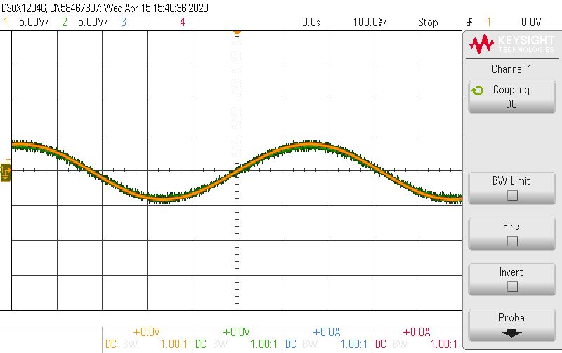
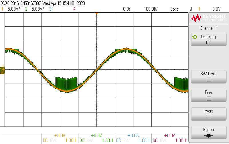
And the output of the function generator and the value measured by ADS5270 were compared and tested with an oscilloscope through DAC.

As in the first picture, the measurement is well within the ±6V range, but beyond that range, noise is included as in the second picture.

We are wondering if there is a problem with the design of the input circuit composed of OP-AMPs.

Or is there a problem elsewhere?

Thanks a million,

Hyeong-Jin

  • Hi Kim,

    Out of the two waveforms in scope screenshots, I understand that one is signal generator output. What is the other one? Did you connect the ADS5270 digital output (connected to FPGA) as input to a DAC and connected the DAC output to scope channel?

    If this is the case, can you check the digital output in FPGA to verify if the ADC output is okay?

    In the schematic you sent, only circuit of IN1P is shown. How is IN1M connected? Can you share that as well?

    Can you also probe signals on pins IN1P and IN1M directly and send scope screenshots? From this, I want to check if common mode voltage and peak voltage are within the spec. 

    Regards,

    Vijay