Because of the holidays, TI E2E™ design support forum responses will be delayed from Dec. 25 through Jan. 2. Thank you for your patience.

This thread has been locked.

If you have a related question, please click the "Ask a related question" button in the top right corner. The newly created question will be automatically linked to this question.

ADS8861: Direct compatibility between LMH32401 and ADS8861

Part Number: ADS8861
Other Parts Discussed in Thread: LMH32401, , ADS8881, ADS8860, REF6045, REF6033, REF6041, REF6030, REF6025

Hi!

My design consists in detecting a light by a photodiode which I will place at the input of the LMH32401 device. At the output of the differential LMH32401 I will connect a differential ADC with SPI interface. Note that the ADC must be differential and also equivalent to a 100 Ohms load because according to his datasheet the LMH32401 is designed to drive at 100 Ohms load. Thank you for advising me an ADC who respect these conditions.

I chose ADS8861  but I am not sure that they are compatible directly, ie if I can connect them directly, knowing that the LMH 32401 is made to drive a load 100 Ohms. What do you think?

If you find that these two devices (LMH32401 and ADS8861) are incompatible, please advise me a differential TIA and a differential ADC with which I can realize my design. Note that I prefer to use differential devices to minimize common mode noise.

  • Hello Andrianirina,

    The LMH32401 should have no issues driving the ADS8861 inputs.

    I took a look at the LMH32401 datasheet.  You do not need a 50ohm load if the amplifier and ADC are located near each other on the same board.  The gain will need adjusted, but otherwise, it should work well without the 50ohm input load.  (Refer to equation 2 in the LMH32401 d.s.)

    You may not need any additional components, but below is how I would design the board.  R1/R2 could be 0ohm resistors, R3/R4 not installed, and C1 may be desirable to reduce the broadband noise.

    Regards,
    Keith Nicholas
    Precision ADC Applications

  • Hello Keit,


    Thank you very much for your email which cheers me up. You are my savior (-:


    You won't believe me if I tell you that what you sent is exactly the design I made, with R10 = R20 = 10Ohms, R3 / R4 not installed, and C1 = 750nF. I will comply with the values ​​you have given.


    I was concerned that the sample rate for the ADS8861 is not fast enough to achieve the full bandwidth of the LMH32401. But, if you confirm to me that it is OK, I am reassured. In any case you are the specialist.


    I take this opportunity to ask you for clarifications concerning the LMH32401 datasheet and more particularly the VOCM, VOD and IDC_EN pins. Please tell me the roles of these pins and tell me the values ​​to which they must be set, depending on the case.


    Always counting on your kind collaboration and your response,


    Best regards.

  • Hello Andrianirina,

    Yes, go ahead and include those components for maximum flexibility.

    However, your statement below needs to be addressed:

    I was concerned that the sample rate for the ADS8861 is not fast enough to achieve the full bandwidth of the LMH32401.


    What is the bandwidth of the signal that you need to measure?  The ADS8861 is limited to 1Msps, which will limit the maximum frequency that you can measure to 500kHz.  In addition, if you expect higher frequency signals than 500kHz, then you will get aliased versions in the converted readings.  This may require a much more complex active filter.  The LMH32401 has a bandwidth of 200-450MHz depending on gain.  If you need to measure much higher frequencies, then the ADS8861 is not suitable, and you would need to look at an ADC with much higher sampling rate (Fsample>=2*Finput).  In other words, if you wanted to support the maximum bandwidth of the LMH32401 at 450MHz, you would need an ADC sampling rate greater than 1Gsps.

    I am not the expert for the LMH32401, but I can provide some guidance.

    1. VOCM; This pin sets the output common mode voltage that the ADC inputs require.  If using the ADS8861 with a 3V reference, then the VCOM would need set to 1.5V to meet the ADS8861 input requirements.  If using a high speed ADC (>100MSPS), then 1.2V may be more appropriate, but the exact voltage depends on the ADC that you are using.

    2.  VOD;  This pin adds an offset voltage when using a photo-diode that sinks current.  It is used to properly scale the signal for the ADC inputs.

    3.  IDC_EN:  This is an internal DC servo loop that rejects any low frequency DC signals.  It effectively acts like a high pass filter to the photodiode input currents, with a high-pass cut-off frequency of 100kHz.

    Regards,
    Keith

  • Dear Keith,

    Dear X,

    Thanks for your kind reply.

    The acquisition frequency is 100KHz maximum, so I think I will be comfortable with the ADS8861 which is limited to 1Msps. Is not it? If so, I can keep the LMH32401 and the ADS8861.

    Please tell me in the LMH32401 datasheet the paragraph that talks about the ADC input requirement and that leads to the VOCM setting of the LMH32401.

    When you talk about the ADS8861 with a 3V reference, which reference are you talking about? Is this ADS8861 pin 1?

    If ADS8861 pin 1 (REF) is 3.3V, what voltage should I set VOCM to?

    According to the VOCM datasheet is set by default to 1.1V when left open. Will I be able to leave it open or link it to GND via capacitor?

    As the lights that will be picked up by the photodiode will vary in intensity, do I understand then that I should apply different voltage to the VOD terminal depending on the light?

    Counting on the speed of your response,

    Best regards.

  • Hello Andrianirina,

    Yes, since your maximum input frequency is 100kHz, the ADS8861 can easily support this and should work with the LMH32401.  You will probably want to sample at 1Msps in this case.

    The ADS8861 has a typical input common mode voltage of Vref/2.  If using a 3.3V reference (Pin1 ), then you would want to set this to 1.65V.  The ADS8861 common mode does allow it to vary from 0V to Vref, but to get the full scale input of +/-3.3V differential, you will want to set this to 1.65V.  Please refer to Table 4 in the ADS8861 datasheet and the Analog Input discussion for more details.

    In order to set Vocm to 1.65V (when using a 3.3V reference voltage on pin 1 of ADS8861), you will need to drive the pin of LMH32401 to this voltage using a voltage divider from Vref and a buffer.  Take a look at the evaluation board for the ADS8881 (18b version) that shows how to design the reference, as well as the Vref/2=1.65V circuit.

    https://www.ti.com/lit/ug/sbau281a/sbau281a.pdf

    Since your input frequency is low, 100kHz or less, you do not want to use the IDC_EN feature.  Regarding the VOD, this depends on the specifics of your photodiode.  It is only used if your photodiode sinks current.  Assuming this is your setup, then the specific value depends on the output current range of your photodiode that you want to capture, as well as the gain setting, and the reference voltage used with the ADC.

    Regards,
    Keith

  • Dear Keith,

    Thank you again for the speed of your response and your precious details and clarification.

    Is it with the circuit below that I will be able to get Vref / 2 = 1.65V? Note that VREF = 3.3V and AVDD = 5V.

    What is the component that I have marked with a red question mark and what is its value?

    I would like to follow the diagram in the LMH32401 datasheet (on the first page and in section 7.2), that is why I will choose a photodiode that absorbs current. Why does the specific value of VOD depend on the output current range of my photodiode, as well as the gain setting and reference voltage used with the ADC? In practice, how can this value be determined knowing that I am going to capture different types of light with my photodiode in the 350 to 110nm wavelength range? Can you give me an example of a calculation?
    Why can't I put VOD on GND directly?

    Finally, can I set IDC_EN to GND?

    I beg you to answer me because I plan to work this weekend to finish.
    Always counting on your usual collaboration and the speed of your response,

    Best regards.

  • Dear Keith,

    Thank you again for the speed of your response and your precious details and clarification.

    Is it with the attached fileCircuit.docx that I will be able to get Vref / 2 = 1.65V? Note that VREF = 3.3V and AVDD = 5V.

    What is the component that I have marked with a red question mark and what is its value?

    I would like to follow the diagram in the LMH32401 datasheet (on the first page and in section 7.2), that is why I will choose a photodiode that absorbs current. Why does the specific value of VOD depend on the output current range of my photodiode, as well as the gain setting and reference voltage used with the ADC? In practice, how can this value be determined knowing that I am going to capture different types of light with my photodiode in the 350 - 110nm wavelength range? Can you give me an example of a calculation?
    Why can't I put VOD on GND directly?

    Finally, can I set IDC_EN to GND?

    I beg you to answer me because I plan to work this weekend to finish.
    Always counting on your usual collaboration and the speed of your response,

    Best regards.

  • Hello Andrianirina,

    Regarding your attached circuit, DNP stands for Do Not Populated.  This resistor is not populated on the normal board, and is optional if the amplifier U4 is not installed.  In order to generate Vref/2=1.65V, R23 and R21 should be set to 10kOhm.

    Regarding the use of VOD, take a look at figures 39 and 40 in the LMH32401 datasheet.  In order to scale the voltage range for the ADS8861, the following settings should be used.

    1.  Use Vref=3V.  This is the lowest value of Vref that can be used when powering the input amplifier, LMH32401, from 3.3V, without additional input protection.

    2.  Vref/2=1.5V.  Drive the VOCM pin of LMH32401 with 1.5V in this case.

    3.  When using a photodiode that sinks current, you have two gain's available; 2k or 20k.  This means you can accommodate a full scale input current range of either 0uA->75uA, or 0uA->750uA.  These appear to be limitations inside the LMH32401 due to internal bias voltages.

    4.  In order to maximize the range available, set VOD=0.75V, per figures 39 and 40.

    5.  You do not want to use the IDC feature, since your maximum input frequency is 100khz.  In this case, IDE_EN needs connected to VDD=3.3V.

    Please note that due to the limitations of the LMH32401 output, the maximum output voltage swing is 1.5Vpp (+/-0.75V differential).  Since the reference for the ADS8861 needs set to 3V, you will only get use of 1/4 of its total range.  In effect, your 16b ADC is now only providing 14b of resolution.

    From a bandwidth (and power) perspective, the LMH32401 is much higher than needed.  You may want to consider building your own front-end trans-impedance amplifier, and then connecting this to the input of a single-ended ADC, such as the ADS8860 (single ended version of ADS8861).  The below reference design will provide more flexibility and easily support 100kHz.

    https://www.ti.com/lit/ug/tidu535/tidu535.pdf

    https://www.ti.com/lit/ds/symlink/ads8860.pdf  (Refer to Figure 63 for suggested input amplifier and reference)

    Regards,
    Keith

  • Hello Dear Keith,

    I thank you for your answer and for your explanations.

    I understand that to have Vref / 2, R23 and R21 must be set to 10kOhm. But I still don't understand whether I should install the resistor R15 which is marked DNP or not. If I have to install it what is its value? So if I don't install it, should I just remove this link?

    So that I understand the values ​​of the tensions that you advise me, see attached my design revision 0 and I ask you to:

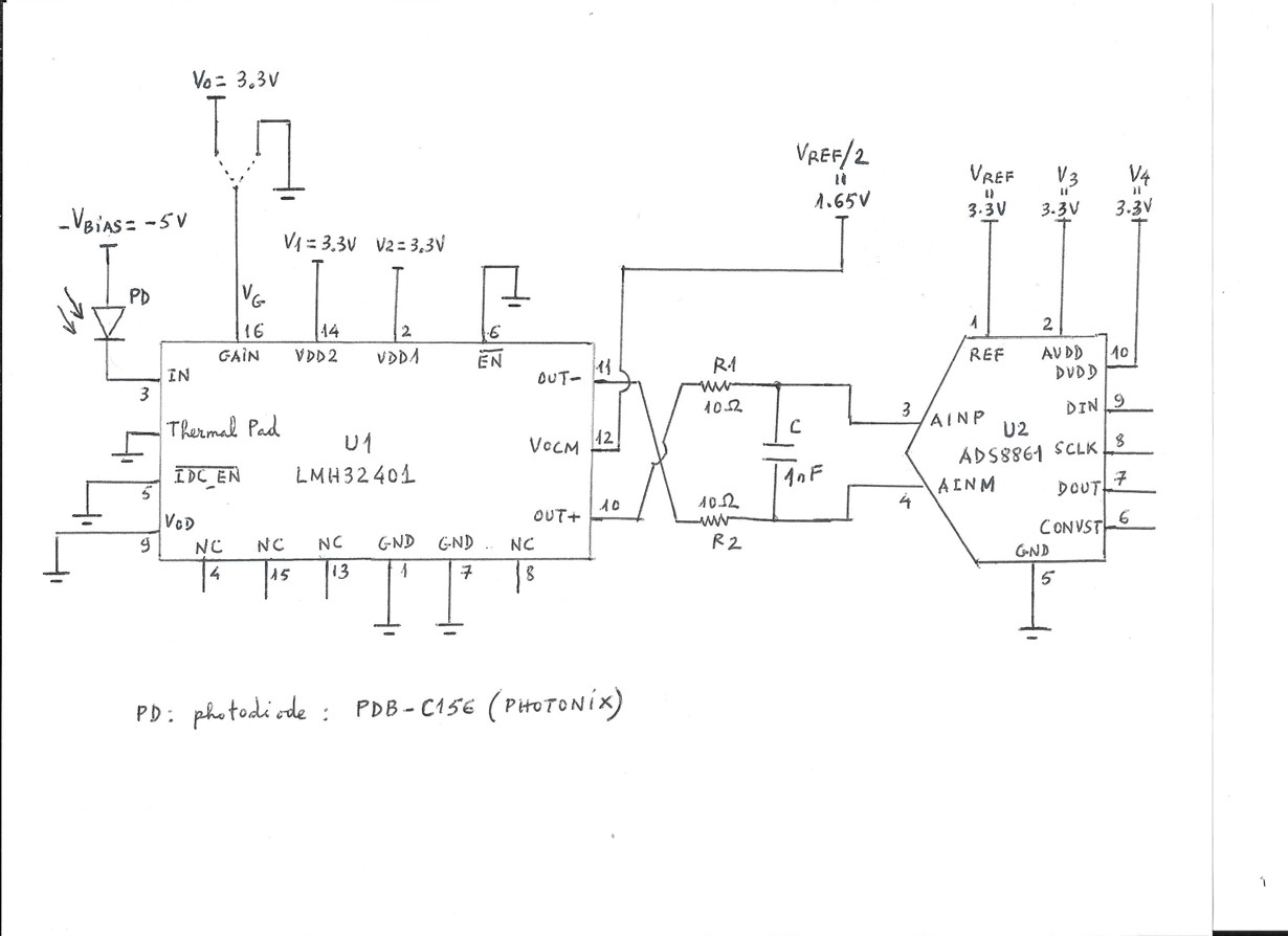
         • Tell me if you approve of it, if not, please review it. Note that the photodiode I am using is that of PHOTONIX P / N: PDB-C156 and I am considering polarizing it negatively with –VBIAS = -5V (voltage level a little high to minimize its capacity).
         • Specify the values ​​of voltages V0, V1, V2, V3, V4, V0D and VREF. For your information, I have set them all to 3.3V, except VOD which is connected to GND.
         • I connect IDC_EN to GND in case the maximum input frequency exceeds 100kHz, knowing that I will be able to go to 500kHz maximum.

    Since VREF needs to be as stable as possible and as little noise as possible, per what is written in the ADS8861 datasheet, I beg you to send me a ready-made circuit, so I can have the VREF voltage. Please also join the circuit that will allow me to have VREF / 2 from VREF.

    Finally, I actually thought about building my own front TIA, then connecting it to the input of an asymmetric ADC, but it is the specifications that require me to choose a differential TIA and a differential ADC .

    Always counting on your precious help who will save me and hoping to receive your answer in a few hours,

    Best regards.

  • Hello Andrianirina,

    You do not need R15 and can remove it from your schematic.

    All supply voltages can be set to 3.3V.  Vod will need to be set to 0.75V.  Vod can be generated using a similar circuit as Vref/2.

    With IDC_EN connected to ground, the LMH32401 will block all input frequencies less than 100kHz.  In other words, if your input frequency was 1kHz, with IDC_EN=GND, you would not be able to measure (the conversion result would be 0). Since your input frequency can range from 0Hz to 100kHz (possibly up to 500kHz), IDC_EN should be connected to 3.3V.

    The ADS8881 (18b version of ADS8861) evaluation board user's guide shows a complete schematic for the reference buffer.

    https://www.ti.com/lit/ug/sbau281a/sbau281a.pdf

    1.  Change REF6045 to REF6033.  U4 can be powered from 3.3V.  REF6033 must be supplied with 3.6V to 5V.

    2. Remove R15, R24.

    3. Change R21, R23 to 10kOhm.

    Also, for the LMH32401, be sure to follow Section 10 (Layout) regarding the supply bypass capacitors.

    Regards,
    Keith

  • Hello Keith,

    Thank you very much again for your answers.

    I have two more final questions, one clarification and one piece of advice.

    1. Questions:

    I understand that to use the full range of my ADC (ADS8861), I need to set Vocm to Vref / 2 (1.65V here), with full differential output from -Vref to + Vref. Is there no problem because the differential output range of LMH32401 is not as high? If this is really a problem, to get the most out of my ATI (LMH32401), can I set the Vocm pin to 1.1V?

    Can you explain to me from equation 1 of section 7.3.4 of the LMH32401 datasheet or another justification how you obtained the 0.75 V value that you recommend for VOD?

    2. Request for clarification:

    By removing R15, I also remove the link between the input and the output of the device OPA33. Is it true?
    By removing R24, should I connect the SS terminal of the REF6033 device to GND or leave it open?


    3. Request for advice:

    In my project, I will use my photodiode to detect lights in the 350 to 1100nm wavelength range, while keeping the same circuit. Can you suggest me a photodiode that is compatible with the TIA and ADC that I have already chosen?

    Finally, I want to inform you that I have already designed several circuits that are less complex than I will need for my project (power supplies, etc.) and I have always used IT devices because I am satisfied with them. This is why I keep asking you questions, so that I can still choose IT devices.

    Always counting on your usual collaboration and your quick response,

    Best regards.

  • Hello Keith,

    I'm resending this email in case you haven't received it.

    Thank you very much again for your answers.

    I have two more final questions, one clarification and one piece of advice.

    1. Questions:

    I understand that to use the full range of my ADC (ADS8861), I need to set Vocm to Vref / 2 (1.65V here), with full differential output from -Vref to + Vref. Is there no problem because the differential output range of LMH32401 is not as high? If this is really a problem, to get the most out of my ATI (LMH32401), can I set the Vocm pin to 1.1V?

    Can you explain to me from equation 1 of section 7.3.4 of the LMH32401 datasheet or another justification how you obtained the 0.75 V value that you recommend for VOD?

    2. Request for clarification:

    By removing R15, I also remove the link between the input and the output of the device OPA33. Is it true?
    By removing R24, should I connect the SS terminal of the REF6033 device to GND or leave it open?


    3. Request for advice:

    In my project, I will use my photodiode to detect lights in the 350 to 1100nm wavelength range, while keeping the same circuit. Can you suggest me a photodiode that is compatible with the TIA and ADC that I have already chosen?

    Finally, I want to inform you that I have already designed several circuits that are less complex than I will need for my project (power supplies, etc.) and I have always used IT devices because I am satisfied with them. This is why I keep asking you questions, so that I can still choose IT devices.

    Always counting on your usual collaboration and your quick response,

    Best regards.

  • Hello,

    The output pins of the LMH32401 are limited from 0.39V to 2.87V max.  Setting the VOCM to 1.65V allows for the maximum swing.

    There are different combinations of VOCM and VOD that will likely work.  However, keeping everything centered (VOCM=1.65V, VOD=0.75V) provides the most margin.

    Equation 1 in the datasheet takes into account the output resistance (20ohm) and the nominal load resistance (100ohm).  In other words, the gain on the VOD pin is adjusted to give 0.75V output offset when VOD=0.75V, and RL=100.  If Rl is a different value from 100ohm, you can use this equation to calculate the proper VOD value to get a desired output offset.

    For your second question, yes, simply delete R15 resistor from the schematic.  (No component or connections)  For R24, leave the SS terminal REF6033 floating, or no connection.

    The below equations may help to better understand the relationship between the input current from the photodiode, the output voltage, and VOD.

    Vodiff-unloaded: The differential output voltage with no external load (Rl=infinity)

    Vodiff-loaded:  The differential output voltage with external load resistor Rl.

    Ipd: Photodiode current

    G: Gain, either 2k or 20k

    Vodiff-unloaded = 1.2*G*Ipd + 1.2*Vod

    Vodiff-loaded = Rl/(Rl+20)*1.2*G*Ipd + Rl/(Rl+20)*1.2*Vod

    If Rl=100ohm, then Vodiff-loaded simplifies to:

    Vodiff-loaded = 100/(100+20)*2.4*G*Ipd + 100/(100+20)*1.2*Vod = G*Ipd + Vod

    Regarding your photodiode question, I cannot provide any suggestions on this.  I suggest you contact the photodiode manufacturer for help on this subject.

    Regards,
    Keith

  • Hello,

    Thank you for your answer and your explanation.

    Regarding the SS pin of the REF6033 device, its datasheet defines it as the short circuit current limit pin and recommends connecting it to a resistor to set the output short-circuit current limit, otherwise to connect it to VIN pin for highest current limit. Is it okay if left open?

    I understand your Vodiff-loaded equation = RL / (RL + 20) * 1.2 * G * Ipd + RL / (RL + 20) * 1.2 * Vod. In our case, what would be the value of RL because we have the ADS8861 as a load? Why do you say VOD = 0.75V is the right value?

    I'm really sorry to ask you all these questions because I would like to understand.

    Thanks for your patience with me.

    Best regards.

  • Dear Keith,

    Continuation of my previous email.

    According to his datasheet, the short-circuit current limit (ISC) of the REF60xx family of devices is adjusted by connecting a resistor (RSS) on the SS pin. The short-circuit current limit when the REF60xx device is sourcing current can be calculated by using the Equation 4.

    Also, the short circuit current limit when the REF60xx device is sinking is calculated by using the Equation 5.

    Finally, the recommended output current of the REF60xx also depends on the resistor connected to the SS pin. The recommended output current (sourcing and sinking) for the REF6025, REF6030, REF6033 and REF6041 is given by Equation 6.

    So, unless I am mistaken, we cannot leave the SS pin open. Please correct me if I am wrong and explain to me why.

    Please answer me today if possible.

    Best regards.

  • Hello Andrianirina,

    Good catch!  You are correct about the REF60xx family.  This pin does need a resistor; a typical value for the resistor is 120kOhm.

    Regarding Vod, the maximum input current range with G=20k is 0uA to 75uA.  This translates to an output differential voltage from 0V to 1.5V (with external Rl=100ohm).  The input range of the ADS8861 is +/-Vref, so in general, you can set the differential voltage to zero volts at 1/2*Input range.  In this case, 1/2*1.5V=0.75V.

    However, since the input range of the ADS8861 will be +/-3.3V, you could connect VOD to ground, VOD=0V, and then the output differential voltage will range from 0V to 1.5V, which is still inside of the ADS8861 input voltage span.  The minimum output voltage on the LMH32401 is about 0.4V.  This will set the minimum VOCM voltage to VOCM=1.5/2+0.4=1.15V.

    Regards,
    Keith

  • Dear Keith,

    I am not tired of thanking you yet.

    In conclusion for, I therefore connect the VOD pin of LMH32401 to the GND and I apply a voltage of (Vref / 2) = 3.3V / 2 = 1.65V on the VCOM pin. Am I right?

    Thank you for responding to me today.

    Best regards.

  • Hello Andrianirina,

    Yes, for your use case, that will work.  VOD=0V, VOCM=1.65V.

    Regards,
    Keith

  • Dear Keith,

    I am coming back to you to be sure of what we decide.

    Won't connecting VOD to GND reduce the output generated by the LMH32401 to half?

    If I am not mistaken if we keep the VOD pin open, the device will provide 510mV to the VOD pin internally. Why not leave it VOD open?

    Why did you give up connecting VOD to a voltage of 0.75V?

    Finally, are you sure that VOCM = VREF / 2 = 1.65V is not too high compared to the output level of LMH32401? So this is better compared to VCOM left open, in which case the default will be 1.1V?

    Please anwer me urgently.

    Thank you so much.

  • Hello Andrianirina,

    Since you are using less than 1/4 of the full scale input range of the ADS8861 (6.6Vpp full scale input), with the output of LMH32401 limited to 1.5Vpp, you have multiple options on where to set VOCM and VOD.

    In any case, if you want to set everything in the 'middle', where you have the most margin, then setting VOCM to 1.65V (optimized for the ADS8861 input range) and VOD to 0.75V (Optimized for the LMH32401 internal bias point) will achieve this.

    Regards,
    Keith

  • Hello Keith,

    Thank you for your reply.

    So you suggest me in conclusion to make VOCM = 1.65V and VOD = 0.75V? Please let me know.

    I beg you to justify me why this value of 0.75V for VOD? Where does this value come from?

    Please answer me now if possible.

    Best regards.

  • Dear Keith,

    In conclusion, you therefore advise me VOD = 0.75V and VOCM = 1.65V. That's right?

    Thank you for explaining to me how you fixed this VOD = 0.75V because I don't understand.

    Counting on your response tonight.

    Best regards.

  • Hello Andrianirina,

    Yes, that is correct.  Although you could do it either way, I always try to design with the most margin possible.

    Regards,
    Keith

  • Hello Keith,


    You wrote in one of your messages: Regarding Vod, the maximum input current range with G=20k is 0uA to 75uA.  This translates to an output differential voltage from 0V to 1.5V (with external Rl=100ohm).  The input range of the ADS8861 is +/-Vref, so in general, you can set the differential voltage to zero volts at 1/2*Input range.  In this case, 1/2*1.5V=0.75V.


    So VOD = 0.75 V will be for a load RL = 100 Ohms.

    What will my equivalent load be in my case because it (RL) will certainly be different from 100 Ohms?

    With this equivalent load is VOD = 0.75V still correct?

    Please answer me this morning if possible.

    Best regards.

  • Hello Andrianirina,

    Please refer to equation 1 in the LMH32401 datasheet. 

    For example, if Rl=1000ohm, and the desired Vod=0.75V, then:

    0.75=1.2*VOD*(1000/(1000+20))

    VOD=0.6375V applied to pin 9 will result in an output offset voltage of 0.75V.

    Regards,
    Keith

  • Hello Keith,

    Thank you for your reply.

    I believe there is an error in writing this equation in the LMH32401 datasheet because the denominator should be (RL + 20 Ohms) but not (RL x 20 Ohms). Am I right?

    Finally, what voltage should I apply on pin 9 of LMH32401: 0.6375V or 0.75V?

    I beg you to answer me now as I am in the process of finalizing my design.

    Best regards.

  • Dear Keith,

    Forget my previous question. My real question is the following: I do not know RL in my case because it is formed by the circuit (R, L) and the ADC installed after the LMH32401. How did you get the VOD value = 0.75V to be applied to pin 9 of the LMH32401 from this equation, when RL is different from 100 Ohms? Will the 0.75V value be fixed for my application or is it possible that I will have to change it?

    Best regards.

  • Hello Andrianirina,

    We want to target an offset on the output of 0.75V.  For the ADS8861, I do not think you need addtional load (Rl) resistors.  In this case, the voltage applied to the Vod pin will have a gain of 1.2.  

    In order to get 0.75V offset on the output pins, Vod should be set to:

    Vod=0.75V/1.2=0.625V.

    Regards,
    Keith