This thread has been locked.

If you have a related question, please click the "Ask a related question" button in the top right corner. The newly created question will be automatically linked to this question.

ADS1114: ALERT/RDY Pin for Continuous conversion mode?

Part Number: ADS1114

Hello,

I'm kind of new to ADS1114 and wanted to sample an ADC value on continuous conversion mode.

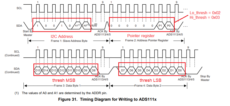
I understand for that I need to set MSB of Hi_Thresh register and L_thresh register as 1 and 0 respectively.

However, I do not understand on how to change it? Is it in the Config register somewhere? I'm sorry for a silly question.

Also,

Does that mean that the output of ADS is sent to the MCU only if it acknowledges/reads the RDY pin. I do not understand that part.

Register values:

unsigned char buffer_Config_Reg[3] = {0x01, 0x80, 0xE1};
unsigned char buffer_Addr_Ptr_Reg[1] = {0x00};

Thanks in advance!

  • Yaagyanika,


    Using the digital comparators isn't absolutely necessary, but they are useful if you want to know when conversions are completed. To ensure that the ALERT/RDY pin trips on every conversion, you would set the high threshold lower than the low threshold. You would also need the comparator to assert after one conversion.

    The threshold register values are the ADC conversion data values where they trip the comparator. For example if the Hi_thresh register is set to 0x3FFF, and the ADC output is 0x4000, then the input voltage is at half positive full scale and the comparator sends the alert.

    To program this you would simply need to send a write to the device with the proper I2C address. The next following byte would be the address pointer indicating which device register you want to write to (Lo_thresh register pointer = 0x02, Hi_thresh register pointer = 0x03). The address pointer is followed by the most significant byte of the threshold register followed by the least significant byte of the threshold register.

    Here is the basic write to the ADS1114 threshold register format, it's taken from the datasheet and is basically a 3 byte write to an I2C device (my comments in RED):

    To change the configuration register, the pointer register is 0x01. 

    The ADC output only goes to the MCU when the ADC conversion register is read. This is a five byte transaction, where you write to the device indicating the pointer register = 0x00, and then reading 2 bytes from the ADC. This is shown in figure 30 of the datasheet. The device does not need to acknowledge the ALERT/RDY pin read. It shows an alert any time a new conversion is available. The master could read the ADC conversion register at any time and it will report the last ADC conversion completed.

    Joseph Wu

  • Thank you for relying to my query.

    So you mean, if I want to read the ADC values from the ADS in a continuous manner, I do not need to employ the ALERT/RDY pin?

    I can just use Config Reg, Point to conversion register and then read continuously?

    Thanks in advance!

    Yaagyanika Gehlot

  • Yaaganika,


    You don't necessarily need to use the ALERT/RDY pin to collect data. However, it might be useful if you need to make sure you collect every single conversion from the ADC.

    With this device, the ADC data comes out at a periodic rate. The default setting is 128SPS or 7.8ms. However, there's a variation of ±10%. For collecting the data, the ADC can free-run but, you don't necessarily know when the ADC completes a conversion unless you program the digital comparator to trip each conversion using the ALERT/RDY pin.

    You could use the ALERT/RDY pin to indicate when the conversion completes and read the data before the next conversion completes.

    Or you could just let it run, and read the data at a speed slower than the data rate (if you need to worry about reading the same conversion twice.


    Joseph Wu

  • Joseph,

    Thank you for explanation! I think for my application I'd have to use the ALERT/RDY pin.

    Do I have to write the config register, hi-threshold and low-threshold register each time before I'm reading from conversion register even if the config register is not to be changed?

    Thanks in advance!

    Yaagyanika Gehlot

  • Yaagyanika,

    If you don't have to change the configuration, then you don't need to rewrite the config register for each conversion. With the device in continuous conversion mode, the ADC will just continue to convert data.

    Joseph Wu

  • Joseph,

    Somehow I'm still not being able to read from the ADS1114.

    I'm using STM32F072RBT6 i2c1 as master. If it's okay and not too much trouble, can you please take a look at my code and tell me if I'm doing anything wrong?

    unsigned char buffer_Config_Reg[3] = {0x01, 0x82, 0xF7};	//	Config Reg pointer, MSB of Config Reg, LSB of Config Reg
    unsigned char buffer_Lo_Thresh_Reg[3] = {0x02, 0x00, 0x00};	//	Lo_Thresh pointer, MSB of Lo_Thresh Reg, LSB of Lo_Thresh Reg
    unsigned char buffer_Hi_Thresh_Reg[3] = {0x03, 0xFF, 0xFF};	//	Hi_Thresh pointer, MSB of Hi_Thresh, LSB of Hi_Thresh Reg
    unsigned char buffer_Conv_Reg[1] = {0x00};	
    
    void Begin_Transmission (void)
    	{	
    		HAL_I2C_Master_Transmit(&hi2c1, 0x48<<1, buffer_Config_Reg, 3, 100);	// Write to Config Register with selected FSR
    		HAL_I2C_Master_Transmit(&hi2c1, 0x48<<1, buffer_Lo_Thresh_Reg, 3, 100);	// Low Threshold Register for continuous conversion
    		HAL_I2C_Master_Transmit(&hi2c1, 0x48<<1, buffer_Hi_Thresh_Reg, 3, 100);	// Access High Threshold Register for continuous conversion	
    	}
    
    double Read_Current_Sensor(void)
    	{
    		HAL_I2C_Master_Transmit(&hi2c1, 0x48<<1, buffer_Conv_Reg, 1, 100);	// Pointing to Conversion register
    		HAL_I2C_Master_Receive(&hi2c1,0x48<<1,buffer_receieve,2,100);		// Recieve data from the sensor and store it in buffer[0] and buffer[1]
    		rawADC = buffer_receieve[0]<<8 | buffer_receieve[1];			// Combine 2 8-bit into 1 16bit
    		Curr_Sensor_ADC_Value = ((rawADC * FSR) / 32767); 		        // ((raw * FSR) / ADC Resolution) 
    		return Curr_Sensor_ADC_Value;
    	}
    
    int main(void)
    {
      HAL_Init();
      SystemClock_Config();
      MX_GPIO_Init();
      MX_I2C1_Init();
      
      Begin_Transmission();
      Main_Current = Read_Current_Sensor();
    		
    	while(1)
    	{
    		if (HAL_GPIO_ReadPin (GPIOA, GPIO_PIN_3) == 1)  // GPIO PA3 is ALERT/RDY
    		{
    		         Main_Current = Read_Current_Sensor();
                    }
    	}
    }
    

    Thanks in advance!

    Yaagyanika

  • Oh, I think I forgot to add: 

    float FSR = 4.096; 

    Thanks.

    Yaagyanika.

  • Yaaganika,

    I'm afraid that I'm not very proficient in coding. 

    Instead of looking at code, it's far easier to use an oscilloscope and look at the I2C waveforms for SDA and SCL directly. You should be able to match the waveforms you see to the timing diagrams you can find in Figures 30 and 31 of the datasheet.

    Once you get some scope shots (or something from a logic analyzer), post the images back here and we can try to debug them.

    Joseph Wu

  • Joseph,

    It worked!

    It was a small matter of config register values in COMP_QUE[1:0].

    I had set it as 11 thinking it will enable ALERT/RDY pin. Going through the datasheet I read that to enable the pin COMP_QUE[1:0] needs to be anything BUT 11.

    Thank you so much for your help!

    Yaagyanika.