


Other Parts Discussed in Thread: ADS131E08EVM-PDK
Hello, everyone,
I would like to read out the ADS131E04 with an Arduino Due via SPI. Unfortunately, I have little previous experience, and this is my first project with an SPI communication.
The voltage level of the SPI is 3.3V and should work with the ADC. I set the clock rate for the SPI communication to 4 MHz. The SPI mode is 1 (CPOL = 0, CPHA=1) and I have set "MSB first".
You can see my code below. If I read out e.g. the ID register in the loop, the answer is always 0x00. I have also already read out all registers one after the other. All of them return the value 0x00. I have also recorded the communication with a logic analyzer. The Arduino sends out commands correctly. I believe the timing is appropriate as well. The signals look good with the oscilloscope so far. The voltage levels and timing are good.

If I read out the sampled data continuously, I also get back measured values which are more or less stable. Here is a sample of the measured data and the recording with the Logic Analyzer. The conversion into the voltage is probably incorrect, because I do not yet consider the sign in the calculation. I would be very happy to receive tips on this.
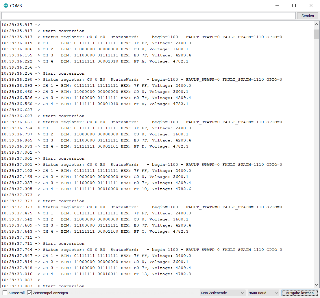

For me, the conclusion is that SPI communication in general works and the ADC is also able to send data that the Arduino understands. Unfortunately, the ADC does not understand the commands I send it, otherwise it would output the register values correctly. Therefore, I think that writing the registers will not work. I have checked the wiring with a colleague several times and found no errors so far. I suspect that maybe the initialization of the ADC is not yet optimal, and I would be glad if someone can help me here. I have followed the procedure from the data sheet (p. 59, Figure 53). I measured the voltage VCAP1 about 1.2V. The toggling of the nDRDY signal with fclk/64 was also visible.
Do you have any hints on what else I can look for? Or did you find errors in my code?
Thank you in advance!
Mandy
Here is the header file:
#define NUM_REGISTERS           ((uint8_t) 21) // 12 Registers are readable and writable (00h to 0Ch and 12h to 14h) --> The addresses 0Dh to 11h cannot be skipped when reading out all registers one after the other (data sheet. pp 38)
#define nCH                     ((int) 4)     // ADC: number of channels

//register addresses
#define ID_reg_add            ((uint8_t) 0x00)
#define CONFIG1_reg_add       ((uint8_t) 0x01)
#define CONFIG2_reg_add       ((uint8_t) 0x02)
#define CONFIG3_reg_add       ((uint8_t) 0x03)
#define FAULT_reg_add         ((uint8_t) 0x04)
#define CH1SET_reg_add        ((uint8_t) 0x05)
#define CH2SET_reg_add        ((uint8_t) 0x06)
#define CH3SET_reg_add        ((uint8_t) 0x07)
#define CH4SET_reg_add        ((uint8_t) 0x08)
#define FAULT_STATP_reg_add   ((uint8_t) 0x12)
#define FAULT_STATN_reg_add   ((uint8_t) 0x13)
#define GPIO_reg_add          ((uint8_t) 0x14)

// registers default values
#define ID_default            ((uint8_t) 0x00)    //unknown, read only
#define CONFIG1_default       ((uint8_t) 0x91)
#define CONFIG2_default       ((uint8_t) 0xE0)
#define CONFIG3_default       ((uint8_t) 0x40)
#define FAULT_default         ((uint8_t) 0x00)
#define CHnSET_default        ((uint8_t) 0x10)
#define CHnPWDN               ((uint8_t) 0x90)
#define FAULT_STATP_default   ((uint8_t) 0x00)    // read only
#define FAULT_STATN_default   ((uint8_t) 0x00)    // read only
#define GPIO_default          ((uint8_t) 0x0F)
#define GPIO_output           ((uint8_t) 0x00)

// SPI control commands (ADC datasheet, p. 35)
#define WAKEUP    0x02  //Wake-up from standby mode
#define STANDBY   0x04  //Enter standby mode
#define RESET     0x06  //Reset the device
#define START     0x08  //Start or restart (synchronize) conversions
#define STOP      0x0A  //Stop conversions
#define OFFSETCAL 0x1A  //Channel offset calibration
#define RDATAC    0x10  //Enable read date continuous mode
#define SDATAC    0x11  //Stop read data continuous mode
#define RDATA     0x12  //Read data by command
#define WREG      0x40  //Write reg
#define RREG      0x20  //read reg

//constants
#define max_23bit   8388607
#define max_15bit   32767
#define max_8bit    255
#define Uref_mV     2400
#define byte_status ((int) 3)
#define byte_data   ((int) 2)


typedef struct{
    uint8_t Begin1100:4;
    uint8_t FAULT_STATP:8;
    uint8_t FAULT_STATN:8;
    uint8_t GPIO:4;
}StatusWord_t;

// function prototypes
void initialize_pins(void);
void startADC(void);
void writeSingleRegister(uint8_t address, uint8_t data);
byte readSingleRegister(uint8_t address);
void readAllRegisters();
void readADC(byte status_reg[], byte data[nCH][byte_data]);
float calcVoltage_mV(uint32_t ADCvalue);
float calcTestVoltage_mV(uint32_t value);
StatusWord_t writeStatusWord(uint32_t ADC_status);

#define PRINTBIN(Num) for (uint32_t t = (1UL<< (sizeof(Num)*8)-1); t; t >>= 1) Serial.write(Num  & t ? '1' : '0'); // Prints a binary number with leading zeros (Automatic Handling)
And here is the main file:
#include "TimeLib.h"
#include <SPI.h>
#include "ADS131E04.h"


unsigned long time;

// Pins
#define ADC_nCS_Pin               10
#define ADC_MasterClk_Select_Pin  11
#define ADC_nDRDY_Pin             12    //active low
#define ADC_Start_Pin             7
#define ADC_nPWDN_Pin             9    // active low
#define ADC_nSysReset_Pin         8    // active low

// SPI
#define SPI_CLOCK_DIV ((int) 21)

// Output mode
boolean RDATA_MODE = true;     //true - RDATA; false - RDATAC
boolean CAPTURE_DATA_MODE = false;   // true - read ADC; false - read Reg in loop

#define pinport PIOB
#define pinmask (1<<25)   // Arduino pin 2 is port B pin 25 (see www.robgray.com/.../Due-pinout-WEB.png)

// Serial output flags
boolean print_status_word = true;
boolean print_data = true;


// times
const int t_StartADC_us    = 25;     // 25 µs
const int t_measure_us     = 1000000; // 100 ms
const int t_delay_SPI_5_us = 5;       // 5 µs
const int t_delay_SPI_2_us = 2;       // 2 µs

byte ADC_values_nCH[nCH][byte_data];      // 3 byte (24bit) for each channel
byte response_status[byte_status];        // 3 status register
StatusWord_t StatusWord;
int32_t ADC_total=0;
uint32_t ADC_status=0;
int Test_voltage_LOW=78;     // 0...255 --> 0V...3,3V (78 = ca. 1.0V)
int Test_voltage_HIGH=150;     // 0...255 --> 0V...3,3V (50 = ca. 1.5V)

//===========================================
void setup() {
  // put your setup code here, to run once:
  Serial.begin(9600);

  Serial.println(" ======================================= ");
  Serial.println(" ");
  Serial.println("Initialize Pins");

  initialize_pins();


  // start the SPI library:
  Serial.println("Start SPI");


  SPI.begin(ADC_nCS_Pin);
  SPI.setClockDivider(ADC_nCS_Pin,SPI_CLOCK_DIV);
  SPI.setBitOrder(ADC_nCS_Pin,MSBFIRST);         // Most Significant Bit first
  SPI.setDataMode(ADC_nCS_Pin,SPI_MODE1);        // SPI_MODE1 - Clock Polarity (CPOL): 0 - Clock Phase (CPHA): 1 - Output Edge: Rising - Data Capture: Falling

  startADC();

  writeSingleRegister(CONFIG3_reg_add,0b11000000);    // use internal reference buffer, Vref=2.4V
  writeSingleRegister(CONFIG1_reg_add,0b10010100);    // data rate = 24bit, 4kSPS (datasheet, p. 41) --> 1001 0100
  writeSingleRegister(CONFIG2_reg_add,CONFIG2_default);
  writeSingleRegister(CH1SET_reg_add,CHnSET_default);
  writeSingleRegister(CH2SET_reg_add,CHnPWDN);
  writeSingleRegister(CH3SET_reg_add,CHnPWDN);
  writeSingleRegister(CH4SET_reg_add,CHnPWDN);
  writeSingleRegister(GPIO_reg_add,GPIO_output);

  // start test signal
  Serial.println("Start test signal");
  analogWrite(DAC0,Test_voltage_LOW);
  analogWrite(DAC1,Test_voltage_HIGH);

  if (RDATA_MODE==false){
    digitalWrite(ADC_nCS_Pin,LOW); //enable device
    SPI.transfer(ADC_nCS_Pin,RDATAC);
    digitalWrite(ADC_nCS_Pin,HIGH); //disable device
  }
}

void loop() {
  if (CAPTURE_DATA_MODE==false){
  Serial.print("Register ID reg: ")  ;
  Serial.println(readSingleRegister(ID_reg_add),HEX);
  //readAllRegisters();
  }
  else{
    time = micros();
        if ((time % (t_measure_us)) >= t_StartADC_us) {   //start read ADC
          Serial.println("Start conversion");
          digitalWrite(ADC_Start_Pin,HIGH); //start conversion

          readADC(response_status, ADC_values_nCH);


          digitalWrite(ADC_nCS_Pin,HIGH); //enable device

          digitalWrite(ADC_Start_Pin,LOW); //stop conversion


          // print status word
          if (print_status_word){
              Serial.print("Status register: ");
              for (int i=0; i<byte_status;i++){
                Serial.print(response_status[i],HEX);
                Serial.print(" ");

              }

              ADC_status=0;
              ADC_status |= (response_status[0])<<16;
              ADC_status |= (response_status[1])<<8;
              ADC_status |= (response_status[2]);
              StatusWord=writeStatusWord(ADC_status);
              Serial.print(" StatusWord: ");
              Serial.print(" ");
              Serial.print(" - begin=");
              Serial.print(StatusWord.Begin1100,BIN);
              Serial.print(" - FAULT_STATP=");
              Serial.print(StatusWord.FAULT_STATP,BIN);
              Serial.print(" FAULT_STATN=");
              Serial.print(StatusWord.FAULT_STATN,BIN);
              Serial.print(" GPIO=");
              Serial.print(StatusWord.GPIO,BIN);

              Serial.println();
          }

          if (print_data){
            // print channel data
            for (int i=0; i<nCH;i++){
                ADC_total=0;
                if (byte_data==2) {
                  ADC_total |= (ADC_values_nCH[i][0])<<8;
                  ADC_total |= (ADC_values_nCH[i][1]);
                 // if( ((ADC_total & 0xffff) & (0x8000))) {
                 // ADC_total = ADC_total|0xffff0000;
                 // }
                }
                else if (byte_data==3) {
                  ADC_total |= (ADC_values_nCH[i][0])<<16;
                  ADC_total |= (ADC_values_nCH[i][1])<<8;
                  ADC_total |= (ADC_values_nCH[i][2]);
                  //if( ((ADC_total & 0xffffff) & (0x800000))) {
                  //ADC_total = ADC_total|0xff000000;
                 // }
                }
              Serial.print("CH ");
              Serial.print(i+1);
              Serial.print(" - BIN: ");
              PRINTBIN(ADC_values_nCH[i][0]);
              Serial.print(" ");
              PRINTBIN(ADC_values_nCH[i][1]);
              if (byte_data==3){
                Serial.print(" ");
                PRINTBIN(ADC_values_nCH[i][2]);
              }
              Serial.print(" HEX: ");
              Serial.print(ADC_values_nCH[i][0],HEX);
              Serial.print(" ");
              Serial.print(ADC_values_nCH[i][1],HEX);
              if (byte_data==3){
                Serial.print(" ");
                Serial.print(ADC_values_nCH[i][2],HEX);
              }
              Serial.print(", Voltage: ");
              Serial.print(calcVoltage_mV(ADC_total),1);
              Serial.println();
            }
          }

          Serial.println();

          //Test_voltage=random(0,255);
          //analogWrite(DAC0,Test_voltage);
          //Serial.print("Test Voltage: ");
          //Serial.println(calcTestVoltage_mV(Test_voltage),1);

          delayMicroseconds(20);

        }
  }
}

void initialize_pins(void){

  // initialize the  data ready and chip select pins:
  pinMode(ADC_nDRDY_Pin, INPUT);
  pinMode(ADC_nCS_Pin, OUTPUT);
  pinMode(ADC_Start_Pin, OUTPUT);
  pinMode(ADC_nPWDN_Pin, OUTPUT);
  pinMode(ADC_nSysReset_Pin, OUTPUT);
  digitalWrite(ADC_nSysReset_Pin,LOW);
  digitalWrite(ADC_nCS_Pin,HIGH); //disable device
}

void startADC(void){
  digitalWrite(ADC_Start_Pin,HIGH);
  delayMicroseconds(10);

  digitalWrite(ADC_nPWDN_Pin,HIGH); //power down disabled
  delayMicroseconds(20);

  delayMicroseconds(1);
  digitalWrite(ADC_nSysReset_Pin,HIGH); //System reset disabled
  delay(150);
  //SPI.transfer(ADC_nCS_Pin,WAKEUP);
  //delay(1);
  SPI.transfer(ADC_nCS_Pin,SDATAC);
  delay(1);
  digitalWrite(ADC_nSysReset_Pin,LOW); //System reset disabled
  delayMicroseconds(1);
  digitalWrite(ADC_nSysReset_Pin,HIGH); //System reset disabled
  delayMicroseconds(10);
  digitalWrite(ADC_nCS_Pin,LOW); //enable device
  delayMicroseconds(10);
  digitalWrite(ADC_Start_Pin,LOW);

  //SPI.transfer(ADC_nCS_Pin,RESET);
  SPI.transfer(ADC_nCS_Pin,SDATAC);
  delayMicroseconds(5);
  SPI.transfer(ADC_nCS_Pin,STOP);
  delay(10);
  digitalWrite(ADC_nCS_Pin,HIGH); //disable device
}

void writeSingleRegister(uint8_t address, uint8_t data){

  digitalWrite(ADC_nCS_Pin,LOW); //enable device

  SPI.transfer(ADC_nCS_Pin,WREG|address,SPI_CONTINUE);
  delayMicroseconds(t_delay_SPI_5_us);
  SPI.transfer(ADC_nCS_Pin,0x00,SPI_CONTINUE);
  delayMicroseconds(t_delay_SPI_2_us);
  SPI.transfer(ADC_nCS_Pin,data);
  delayMicroseconds(t_delay_SPI_2_us);

  digitalWrite(ADC_nCS_Pin,HIGH); //disable device
}

byte readSingleRegister(uint8_t address){
  byte value;

  digitalWrite(ADC_nCS_Pin,LOW); //enable device

  SPI.transfer(ADC_nCS_Pin,RREG|address,SPI_CONTINUE);
  delayMicroseconds(t_delay_SPI_5_us);
  SPI.transfer(ADC_nCS_Pin,0x00,SPI_CONTINUE);
  delayMicroseconds(t_delay_SPI_2_us);
  value = (byte) SPI.transfer(ADC_nCS_Pin,0);
  delayMicroseconds(t_delay_SPI_2_us);
  digitalWrite(ADC_nCS_Pin,HIGH); //disable device
  return value;
}

void readAllRegisters(){
  byte val[NUM_REGISTERS];
  digitalWrite(ADC_nCS_Pin,LOW); //enable device

  SPI.transfer(ADC_nCS_Pin,RREG|0x00,SPI_CONTINUE);
  delayMicroseconds(t_delay_SPI_5_us);
  SPI.transfer(ADC_nCS_Pin,0x14,SPI_CONTINUE);
  delayMicroseconds(t_delay_SPI_2_us);
  for (int i=0;i<NUM_REGISTERS;i++){
    val[i] = (byte) SPI.transfer(ADC_nCS_Pin,0,SPI_CONTINUE);
    delayMicroseconds(t_delay_SPI_2_us);
  }
  SPI.transfer(ADC_nCS_Pin,0);
  delayMicroseconds(t_delay_SPI_2_us);
  digitalWrite(ADC_nCS_Pin,HIGH); //disable device
  for (int i=0;i<NUM_REGISTERS;i++){
    Serial.print("Register ");
    Serial.print(i);
    Serial.print(": ");
    Serial.println(val[i],HEX);
  }
}

void readADC(byte status_reg[], byte data[nCH][byte_data]){

  while (digitalRead(ADC_nDRDY_Pin)) { }  // wait until nDRDY is 0 to read data

  digitalWrite(ADC_nCS_Pin,LOW); //enable device
  delayMicroseconds(1);
  if (RDATA_MODE==true){
    SPI.transfer(ADC_nCS_Pin,RDATA,SPI_CONTINUE);
    delayMicroseconds(t_delay_SPI_5_us);
  }

  //status word
  for (int i=0; i<byte_status;i++){
    status_reg[i] = SPI.transfer(ADC_nCS_Pin,0,SPI_CONTINUE);
    delayMicroseconds(t_delay_SPI_2_us);
  }

  //data
  for (int i=0; i<nCH;i++){
    for (int k=0;k<byte_data;k++){
        data[i][k]= SPI.transfer(ADC_nCS_Pin,0);
        delayMicroseconds(t_delay_SPI_2_us);
    }
  }
  digitalWrite(ADC_nCS_Pin,HIGH); //disable device
  delayMicroseconds(1);
}

float calcVoltage_mV(uint32_t ADCvalue){
  float voltage;
  if (byte_data==2) {
     voltage = (float) ADCvalue*Uref_mV/max_15bit;
  }
  else if (byte_data == 3){
     voltage = (float) ADCvalue*Uref_mV/max_23bit;
  }
  return voltage;
}

float calcTestVoltage_mV(uint32_t value){
  float voltage = (float) value*Uref_mV/max_8bit;
  return voltage;
}

StatusWord_t writeStatusWord(uint32_t ADC_status){
  StatusWord_t value;

  for (int i=0;i<4;i++){
    bitWrite(value.Begin1100,3-i,bitRead(ADC_status,23-i));   // first bits must be 1100
  }

  for (int i=0;i<8;i++){
    bitWrite(value.FAULT_STATP,7-i,bitRead(ADC_status,19-i));
  }

  for (int i=0;i<8;i++){
    bitWrite(value.FAULT_STATN,7-i,bitRead(ADC_status,11-i));
  }

  for (int i=0;i<4;i++){
    bitWrite(value.GPIO,3-i,bitRead(ADC_status,3-i));
  }
  return value;
}


)