This thread has been locked.

If you have a related question, please click the "Ask a related question" button in the top right corner. The newly created question will be automatically linked to this question.

DAC80504: What is the read timing for the first bit?

Part Number: DAC80504

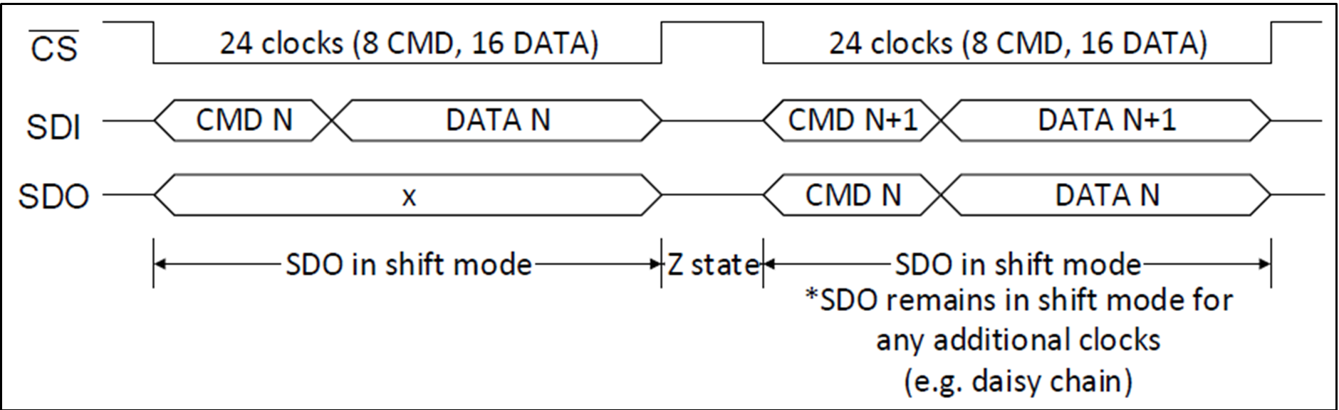
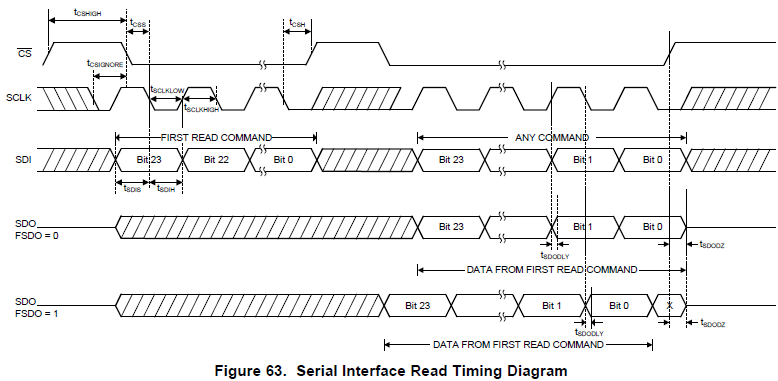
The SBAS871C (August 2017) data sheet illustrates the read timing in Figure 63 but fails to illustrate the start of the read data transaction properly with coordination of CS, SCLK, and read Bit 23..  SCLK is not illustrated properly between the command/data transaction pair; I'm assuming SCLK should be high when CS goes low for both command and data transactions but it's unclear.  There is no SDO tristate illustrated between the command and data.  Will SDO remain driven during CS high?  If FDSO=1, does read bit 23 show up (or remain?) when CS goes low and change to bit 22 after the first falling clock that samples command bit 23?

An illustration from a previous forum question DAC80504: Problems interfacing with DAC80504 shows a more complete timing diagram but with parameters that are not part of the DAC80504 register map.

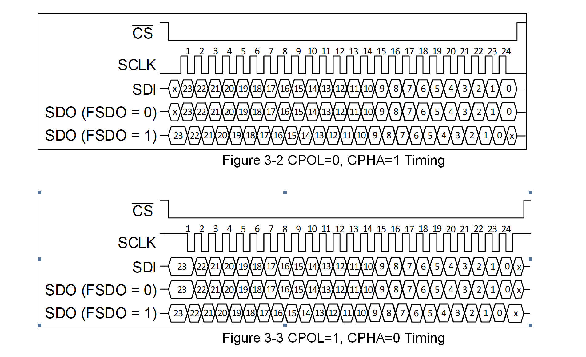
Does one of the two figures above correspond to the operation of the DAC80504?  Are CPOL or CPHA available on the DAC80504?

Many thanks for any insights.

JH

  • Hi,

    CPOL and CPHA is related to generic SPI, not related to device.

    DAC80504 supports SPI mode 1 and 2, corresponding timing diagrams are shown in the post you mentioned.

    When CS is high SDO will be in high Z state. Sorry for not being clear in the datasheet. I will take a note and update the same in our next revision update.

    Please see the read diagram more clearly below.

    SCLK can be high or low depends on the SPI mode you are operating.

    Hope this clarifies your query. Let me know if you need more help.

    Regards,

    AK

  • Are the following assumptions true?

    1) when CS goes low, SCLK can be high or low with tcss defining the required time from CS to the first high-to-low transition of the SCLK.

    2) when FDSO=1, data read bit 23 is valid immediately after CS goes low and changes to bit 22 after the first falling edge of SCLK which also is used to sample the command bit 23 from SDI.

    3) when FDSO=0 and SCLK=1 when CS goes low, SDO data is valid immediately with data bit 23 and changes after the first rising edge of SCLK.

    4) when FDSO=0 and SCLK=0 when CS goes low, SDO data bit 23 becomes (or stays) valid on the first rising edge of SCLK and changes after the second rising edge.

    I'm trying to use one common SPI interface between 4 different TI parts and the implementation details become important, dynamically changing for each device.

    Thanks again,

    JH

  • Hi,

    You are correct on this interpretation. To avoid false operations, CS should toggle with certain timing margins between CS and SCLK for the CS falling edge to first SCLK rising edge (tCSS in product datasheet) and the last SCLK falling edge to CS rising edge (tCSH in product datasheet) in a frame.

    For the read data output operation, the 32 bit input shift register is loaded with 16 LSBs of readback data at the eighth SCLK falling edge after the SYNCn falling edge of the readback command frame. The 8 MSBs are an echo (copy) of the 8 MSBs which were previously shifted in from the readback command frame. Then, at each SCLK rising edge, the SDO is updated. However, if the FSDO (‘fast’ SDO) bit on the CONFIGURATION register is set, the SDO is updated a half-cycle earlier, at each SCLK falling edge. The primary purpose of FSDO is to trade off setup time with hold time with respect to the next device in the chain. FSDO provides a half-cycle more setup time, while reducing hold time. Many applications can benefit from this mode when SDO delay is too large for a desired SCLK frequency. See the figure below.

    See the below figure for FSDO details.

    Regards,

    AK

  • Sincere thanks.  The illustration is much clearer.  Aside from the description in the first line of "CS falling edge to first SCLK rising edge" being inverted - tcss is CS to SCLK falling edge setup - my questions are answered.

    Many thanks!

    JH