


Other Parts Discussed in Thread: ADC12D1000
Hi TI experts,
I have some technical questions on ADC10D1000, as listed below.
1. I see Vcmo is internally buffered. Does TI recommend connecting this pin directly to the common-mode input pin of an fully differential amplifier (FDA), or externally buffering it before connecting it to an FDA?
2. If the Tdiode+- pins are not used, is it OK to leave them floating (not connected)?
3. In typical performance plots shown in datasheet, how many samples are used to perform FFT?
4. The equivalent circuit of CalDly shows that it is a CMOS input pin. Why the recommended pull up/down resistor is 1k Ohm? What are the considerations?
5. If the ADC is operating at DESI mode and 1:4 Demux mode, can I latch DQ and DQd with DCLKI and leave DCLKQ floated (since DCLKI and DCLKQ are always in phase), or terminate DCLKQ with a 100-ohm resistor but not connect DCLKQ to FPGA? If ORI is high indicating VinI is out of range, how do I determine which sample is out of range, since both DI and Did are clocked out at the moment? Are ORQs active in 1:4 Demux mode?
6. Does the part require a specific power supply ramp rate?

7. What is the recommended termination method for the unused AC-coupled input in DES mode? Table 18 says one should tie unused+ to unused-, while the datasheet (AC-coupled Input Signal section, page 60) also mentions that the unused AC-coupled inputs should be connected to ground through capacitors.
8. In both DES and Non-DES modes, the unused DC-coupled inputs should be tied to Vbg, right? Is there any requirement on how should we connect them? For example, should we connect them through traces with a specific characteristic impedance, or through low-impedance planes?
9. How to terminate the unused SPI pins in Non-ECM mode?
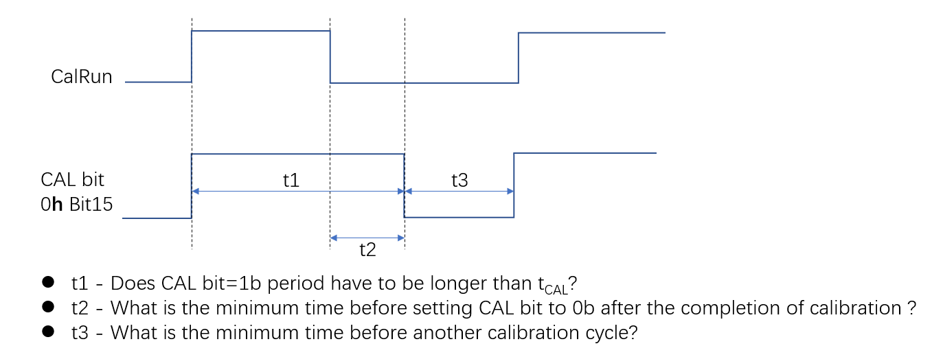
10. What is timing requirement of calibration as shown below?
Looking forward to your reply. Thanks.


