This thread has been locked.

If you have a related question, please click the "Ask a related question" button in the top right corner. The newly created question will be automatically linked to this question.

[FAQ] Delta-sigma ADC anti-aliasing filter component selection

Other Parts Discussed in Thread: ADS124S08

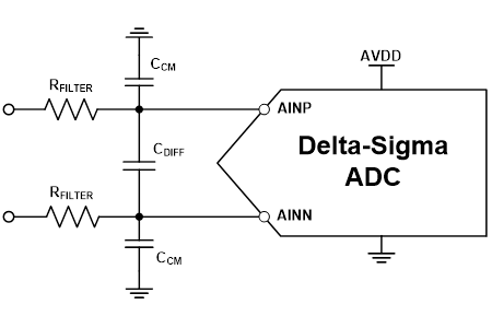
I am trying to develop a system using a low speed delta-sigma ADC for DC-type measurements. How do I select the component values for the anti-aliasing filter?

  • Hello,

    Low-speed delta-sigma ADCs generally require a simple single-pole RC filter to reduce aliasing effects. For differential signals, the filter structure is typically comprised of two filtering paths: a differential filter derived from the combination of both filter resistors, RFILTER, and the differential capacitor, CDIFF; and a common-mode filter derived from combination of one filter resistor, RFILTER, and the common-mode capacitor, CCM. This is shown in Figure 1.

     Figure 1: Anti-aliasing filter structure for low-speed delta-sigma ADC

    [NOTE: for a single-ended input where AINN is referenced to ground, the filter would be comprised of RFILTER and CCM. However, the design guidelines would be the same as those for the differential filter described below.]

    To determine the values of each component in Figure 1, it helps to break the analysis into three parts:

    • How to select the differential filter cutoff frequency
    • How to select the filter resistor value
    • How to select the differential and common-mode capacitor values

    The first two questions can be answered in parallel since their answers do not depend on each other. The third question can be answered using the results from the first two. Moreover, for each question, the ADS124S08 – a 24-bit, 12-ch, 4-kSPS delta-sigma ADC – will also be used as an example data converter to help illustrate how to put these design principles into practice.

    How to select the differential filter cutoff frequency

    The purpose of an anti-aliasing filter is to keep frequency content at or near the ADC’s modulator frequency, fMOD, from aliasing back into the passband, since these frequencies are not natively rejected by the digital filter. As a result, start by choosing a differential filter 3-dB cutoff frequency, fC-DIFF, such that it is 10x to 100x lower compared to fMOD. This results in 20-dB to 40-dB rejection of frequencies around fMOD, respectively. The amount of rejection required depends on the system design goals. To learn more about anti-aliasing filter fundamentals as well as why it is necessary to consider aliasing of the modulator frequency, please review the Precision Labs content on this topic (modules 6.5 and 6.6)

    For the ADS124S08, fMOD is fCLK / 16, where fCLK is the main clock frequency as shown in Figure 2. Given the nominal internal oscillator frequency of 4.096 MHz, fMOD = 4.096 MHz / 16 = 256 kHz. Therefore, for this specific ADC, initially choose fC-DIFF = 2.56 kHz or fC-DIFF = 25.6 kHz to get 40 dB or 20 dB of rejection, respectively.

     Figure 2: ADS124S08 digital filter structure and modulator clock

    While setting fC-DIFF = 2.56 kHz or fC-DIFF = 25.6 kHz to get 20 dB or 40 dB of rejection, respectively, is a good first step, it might be necessary to modify fC-DIFF given the following two conditions:

    1. Ensure that fC-DIFF is greater than the digital filter 3-dB frequency, fC-DIGITAL, at the selected data rate or the RC filter can influence the digital filter characteristic. Choosing fC-DIFF ≥ 10 ⋅ fC-DIGITAL typically reduces any impact the RC filter can have on the digital filter
    2. Ensure that fC-DIFF is not significantly smaller than the ADC output data rate (ODR) or the input signal might not settle before the conversion process begins. Choosing fC-DIFF ≥ ODR is typically sufficient

    For more information about the recommendation in Condition #1, refer to the Precision Labs content cited earlier in this FAQ. For more information about the recommendation in Condition #2, review the application note Calculating Conversion Latency and System Cycle Time for Delta-Sigma ADCs, specifically the section regarding Analog Settling.

    How to select the filter resistor value

    In the system shown in Figure 1, the filter resistor also limits the current into the ADC pin. As such, this resistor is sized to limit the maximum pin input current (IMAX) as shown in the ADC Absolute Maximum Ratings table. To determine the allowable voltage drop across this resistor, use the expected overvoltage conditions seen at the system input (VOV) as well as the turn-on voltage for the ADC integrated ESD protection diodes (VESD). Then, use the following equation to solve for the resistor value, RFILTER:

    RFILTER > (VOV – VESD) / IMAX

    For the ADS124S08, IMAX is 10 mA as shown in table 7.1 in the device datasheet. Moreover, as Figure 3 shows, the ADS124S08 ESD diodes turn on when the input voltage is 300 mV beyond the analog supplies.

     Figure 3: ADS124S08 ESD information

    Finally, using example values of AVDD = 5 V and VOV = 20 V enables the minimum size for RFILTER to be determined:

    VOV = 20 V

    VESD = AVDD + 0.3 V = 5.3 V

    IMAX = 10 mA


    RFILTER > (VOV – VESD) / IMAX = (20 V – 5.3 V) / 10 mA = 1,470 Ω

    Note that this is the absolute smallest value the resistor can be to limit the current into the ADC pins given the system parameters. It is best practice to allow margin on the overvoltage conditions and the maximum current when calculating the resistor size. This ensures a more robust protection circuit that can accommodate any potential system variation. For example, assume a 10% tolerance on VOV as well as a 30% tolerance on IMAX:

     VOV’ = VOV ⋅ 1.1 = 22 V

    VESD = AVDD + 0.3 V = 5.3 V

    IMAX’ = IMAX ⋅ 0.7 = 7 mA

    VOV’ = IMAX’ represent the values of VOV and IMAX including the specified tolerances. These values can then be used to determine the value of RFILTER for this system, RFILTER’:

    RFILTER’ > (VOV’ – VESD) / IMAX’ = (22 V – 5.3 V) / 7 mA = 2,386 Ω

    While no maximum value is given for RFILTER (or RFILTER’), consider the impact ADC leakage currents can have as they flow across larger values of RFILTER. These leakage currents can introduce significant offset errors at the ADC inputs. It is typically acceptable to choose RFILTER to be no larger than 10 kΩ to help minimize these errors, though RFILTER< 5 kΩ is usually sufficient in most cases.

    After calculating RFILTER for the specific system, choose a standard resistor that is equal to or greater than this value.

    How to select the differential and common-mode capacitor values

    After determining the fC-DIFF and RFILTER, use following equation to determine the size of the capacitor for the differential filter, CDIFF:

    CDIFF = 1 / [ 2 ⋅ π ⋅ fC ⋅ (2 ⋅ RFILTER) ]

    The common-mode capacitors, CCM, are then chosen to be 10x to 20x smaller than CDIFF, such that:

    CCM = CDIFF / 10

    or

    CCM = CDIFF / 20

    Given the values for RFILTER and fC-DIFF determined previously, calculate the capacitor values assuming CCM = CDIFF / 10:

    CDIFF = 1 / [ 2 ⋅ π ⋅ fC ⋅ (2 ⋅ RFILTER) ] = 1 / [ 2 ⋅ π ⋅ 2,560 Hz ⋅ (2 ⋅ 1,470 Ω) ] = 21 nF

    CCM = CDIFF / 10 = 21 nF / 10 = 2.1 nF

     That’s all there is to it! You are now ready to apply these design principles to the next project.