This thread has been locked.

If you have a related question, please click the "Ask a related question" button in the top right corner. The newly created question will be automatically linked to this question.

ADS114S08: ADS114S08 Multiple RTDs measurement error

Part Number: ADS114S08

Dear Bob,

Wish you a happy new year. Hope you are doing well.

Currently we are measuring Temperature using ADS114S08 and facing problem for RTD Temperature sensors. Here below I gave you detail description for same.

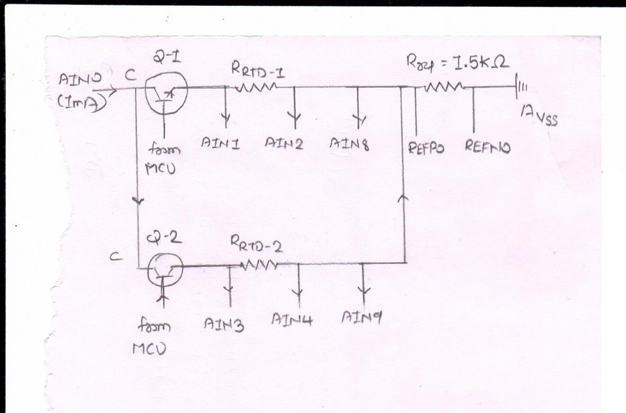
As per "A Basic Guide to RTD Measurements" application note we are using Two-Wire RTD, Low-side reference measurement circuit and Three-Wire RTD, Low-side reference measurement circuit with one IDAC for our temperature measurement.

For First Three Wire RTD measurement register configurations are as follows,

Register details

Data in Hex

REG 01

0x00

REG 02

0x12

REG 03

0xEA

REG 04

0x9C

REG 05

0x12

REG 06

0x07

REG 07

0xF0

REG 08

0x00

REG 09

0x10

Register details

Data in Hex

REG 01

0x00

REG 02

0x28

REG 03

0xEA

REG 04

0x9C

REG 05

0x12

REG 06

0x07

REG 07

0xF0

REG 08

0x00

REG 09

0x10

Three Wire RTD terminal (A-B-b), A connected to AIN1, B connected to AIN2 and b connected to AIN8.

For Second Three Wire RTD measurement register configurations are as follows,

Register details

Data in Hex

REG 01

0x00

REG 02

0x34

REG 03

0xEA

REG 04

0x9C

REG 05

0x12

REG 06

0x07

REG 07

0xF0

REG 08

0x00

REG 09

0x10

Register details

Data in Hex

REG 01

0x00

REG 02

0x49

REG 03

0xEA

REG 04

0x9C

REG 05

0x12

REG 06

0x07

REG 07

0xF0

REG 08

0x00

REG 09

0x10

Three Wire RTD terminal (A-B-b), A connected to AIN3, B connected to AIN4 and b connected to AIN9.

As you can see in configuration registers sets, we are using 1mA Exitation current source both RTD Channels. As per our knowledge we can not pass 1 mA current source to both RTD channels at a same time So we are using transistor as a Switching network. So, at a time only one RTD channel will get current of 1 mA from Source pin.

Our program sequence is as follow,

1)      start the SPI module

2)      configure ADS114S08

3)      wait for Vref to settle

4)      sending START command to start conversion

5)      Turn ON transistor 1 for RTD1 measurement

6)      After taking measurement 1 (voltage reading between AIN1-AIN2) & 2 (voltage reading between AIN2-AIN8) for RTD1 Turn OFF transistor 1

7)      Turn ON transistor 2 for RTD2 measurement

8)      after taking measurement 1 (voltage reading between AIN3-AIN4) & 2 (voltage reading between AIN4-AIN9) for RTD2 Turn OFF transistor 2

9)      repeat step-5 to step-8

Here we are using 1.5k ohms precision resistor as reference resistor. Both RTDs negetive side are connected to same reference network.

Let us update is this methode is correct to check tempeature using RTD on multiple AIN inputs? If this is incorrect then kindly give some circuit information which can help us to measure temperature using same IC for 4 nos. of 3 Wire RTD. We are just checking 2 nos of RTD for trial bases. But our end applocation is to measure temperature using 4nos of RTD only.

If you need any further details then let us know.

Waiting for your prompt response.

Thanks and Regards,

Jehan Patel

  • Hi Jehan,

    I don't have any specific data or information on what you are expecting and the result you are seeing.  Based on the configuration settings I would think that this might be an analog settling issue.  When you change input channels, are you writing registers 0x01 through 0x09 each configuration, or just the required mux changes?  I would suggest only writing the registers that are changing.

    I would also suggest looking at one channel to determine if there is settling or a noise issue.  If you just measure one input channel continuously, does the data always appear the same?  Or do you see a settling behavior in the result at the start of the measurement series?  

    I see that in your register settings that you have changed the built-in delay time after a mux change to the minimum value.  If you have any change in routing and there is capacitance in the signal path, you must make sure that you delay sufficiently for the analog path to settle.  For example, in your sequence of events you wait for the internal reference to settle (3), then issue the Start command (4) which starts the conversion, then you turn on the transistor (5).  This means that you start the conversion with no valid reference and then the current is applied.

    There will also be some path delay when turning off Q1 and turning on Q2.  The conversion should not start until the current path has fully settled.

    Best regards,

    Bob B

  • Hi Bob B,

    Thanks for your quick reply.

    1)      “When you change input channels, are you writing registers 0x01 through 0x09 each configuration, or just the required mux changes? I would suggest only writing the registers that are changing” - as we mentioned in our previous comment, we have to measure temperature using 4 RTDs. So as per data sheet page no. 66 (9.5.3.12), writing to register 0x02 through 0x07 and 0x09 will start new conversion. For that reason we are configuring ADS114S08 every time.

    When we try with changing only analog input MUX setting, for second measurement we just changed INPUT MUX to AIN2 and AIN8. By turning ON transistor Q1 constantly and the measurement result are as follow, actual temperature is 68.8 ˚C and ADS114S08 showing 77.8 ˚C.

    2)      “I would also suggest looking at one channel to determine if there is settling or a noise issue. If you just measure one input channel continuously, does the data always appear the same? Or do you see a settling behavior in the result at the start of the measurement series?” – As per your suggestion we try with single channel by turning ON transistor Q1 constantly and measurement result are as follow, Actual temperature is 68.8 ˚C and ADS114S08 showing 67.7 to 68 ˚C. Here for second measurement we configured all registers ADS114S08 once again. If we change only MUX value then it will be showing incorrect result as mentioned in above point.

    3)      “I see that in your register settings that you have changed the built-in delay time after a mux change to the minimum value. If you have any change in routing and there is capacitance in the signal path, you must make sure that you delay sufficiently for the analog path to settle. For example, in your sequence of events you wait for the internal reference to settle (3), then issue the Start command (4) which starts the conversion, then you turn on the transistor (5). This means that you start the conversion with no valid reference and then the current is applied.”- Thanks for pointing out mistake we have made, now we applying start command after turning ON transistor. But when we turn OFF the transistor after taking measurement 1 & 2. Again turning ON transistor it will showing 86.9 ˚C but actual temperature is 68.8 ˚C. As per datasheet of ADS114S08 page no. 34 (9.3.3.1), 10uF capacitor between REFOUT and REFCOM needs 4.9ms delay. Without this delay we are not getting any result as expected. So let us update is this delay required before stare command or not?

    We want to connect 4 Three Wire RTDs to ADS114S08 with switching of 1mA excitation current for each RTD. So suggest us if any reference circuit is available.

     Please take a look on below code sequence and let us update is there any modifications required or not.

     -         Turning Transistor ON

    -          Configuring all registers of IC for AIN1-AIN2 measurement

    -          4.9 mSec Delay

    -          Start command

    -          RDATA command

    -          Configuring all registers of IC for AIN2-AIN8 measurement

    -          4.9 mSec Delay

    -          Start Command

    -          RDATA command

    -          Turning Transistor OFF

    Thanks and Regards,

    Jehan Patel

  • Hi Jehan,

    It is true that by writing to particular registers the conversion will restart if a conversion is in progress.  I would suggest however that you only write to the registers if the contents will change.  For example, you do not need to write to all of the registers if only the mux is changing.

    I am confused by how your are making your measurements.  Each RTD measurement requires 2 measurements.  One to measure the RTD and the second to measure the lead resistance.  How are you making this calculation?  And instead of giving me temperature converted values, can you give me the code being returned for each of the two measurements?

    As to why you need to write all registers to get the correct result is difficult for me to understand as the only thing that is changing is measurement channels.  All that differs when writing all of the registers is the start of conversion is delayed.  Can you give me a more detailed schematic?  Are you using any analog input filters?

    For the delay for the REFOUT/REFCOM this would only apply to the initial startup as this is for the internal reference only that is used to reference the IDACs.  This should only need to be done at the start.  Any further delay required will depend on the reference settling for the RTD reference when switching channels.

    One further thing I should mention and that is the use of the START command.  If the START command has already been issued previously any additional START command will be ignored unless a STOP command precedes it.  So to actually restart a conversion, you will need to send the STOP command then the START command.

    Best regards,

    Bob B

  • Hi Bob b,

    1) “I am confused by how you are making your measurements. Each RTD measurement requires 2 measurements. One to measure the RTD and the second to measure the lead resistance. How are you making this calculation? And instead of giving me temperature converted values, can you give me the code being returned for each of the two measurements?” – Here measurement value you asked for, When Q1 transistor constant ON measurement 1:0x2C74 to 0x2C94 and measurement 2: 0x156.

    Final value of RTD = Rref * [(measurement 1 – measurement 2) / (32767 * PGA gain)]

    Where, Rref = 1.5 KΩ and PGA gain = 4

    2) “Are you using any analog input filters?” – Yes, we are using analog input filter at analog input side, with 470 Ω filter resistance, 0.01 µF capacitor for common mode filter and 1µF capacitor for differential mode filter. Please find attached file for more details.


    3)  “For the delay for the REFOUT/REFCOM this would only apply to the initial startup as this is for the internal reference only that is used to reference the IDACs. This should only need to be done at the start. Any further delay required will depend on the reference settling for the RTD reference when switching channels.” – Here we are using delay from table 18 which is available in datasheet of ADS114S08 page no.46 (9.3.6.5) for selected data rate. Delay values that mentioned in table 18 are necessary or not. Further delay that you are telling about that is applied after START command or before START command??

    4)  “One further thing I should mention and that is the use of the START command. If the START command has already been issued previously any additional START command will be ignored unless a STOP command precedes it. So to actually restart a conversion, you will need to send the STOP command then the START command.” – We tried with your solution by applying STOP command after START command there no change in result when Transistor Q1 is always ON. Still we did not get correct result when Q1 Transistor is ON for measurement 1 & 2 and remains OFF when measurement not needed.

    When we try with transistor Q1 transistor ON for measurement 1 & 2 and Transistor OFF for when measurement is not needed. The conversion result is as follow, measurement 1:0x3020 to 0x3077 and measurement 2: 0x1A9 to 0x1AB.

    Consider Reference resistor value : 1.5 KΩ

    Thanks and Regards,

    Jehan Patel

    4ch RTD.pdf

  • Hi Jehan,

    The schematic shows a lot more capacitors than I would have expected.  Are all these capacitors in circuit?

    Even with the values you mentioned there is considerable analog settling.  You need to consider all of the resistance and capacitance for each portion of the circuit involved.  For the reference alone you need to consider the complete path of the RTD as well as the input filtering.  The number of time constants for analog settling is based on achieving 1/2 LSB of certainty and for a 16-bit device will be about 11.78.

    So calculate the time constant (R*C) for each portion of the circuit (differential input is 2*R*C), and for longest portion calculate the time required for settling.  For a 1uF cap and two 470 Ohm resistors the time constant is 940us, and for full settling would be 940us * 11.78 (11.1ms).

    Best regards,

    Bob B

  • Dear Bob,

    Thanks for the information.

    Can you please explain us how we can calculate exact delay required for our circuit?

    Please provide us some datasheet or reference manual or link for better understanding.

    Because this things are not mentioned in ADS114S08 Datasheet.

    Kindly help us to build proper 4nos of 3 Wire RTD circuit with all kind of protection circuit implementation.

    We made this circuit from one of your application notes. But there are only thermocouple protection circuits are available and we are looking for RTD networks also.

    We are following below link for protection circuit implementation.


    We can modify our circuit as per your suggestions. We need less conversation delay time with full protection circuit and best accuracy which can beat any noisy environment.

    Thanks and Best Regards,

    Jehan Patel

  • Hi Jehan,

    I understand your situation, but it is not for me (or TI) to decide how you should design your circuit.  We have some reference designs, but most of the time the customer designs are unique in some way.

    As a totally different type of example, let's say I wanted the fastest automobile possible, with the most comfortable ride, that could traverse any terrain and operate with the lowest cost with respect to miles per gallon.  As examples I can see that there are many different automobile manufacturers that I can pattern my design after, but in the end I would have to make some decisions and be more specific as to my design criteria.

    As a part of your design, there will be certain criteria that become very important in the design process.  This will include the rate at which you need to measure all four RTDs.  Also as a part of this design, you will need to specify the level of noise filtering required.  The ADS114S08 has noise tables with respect to PGA gain that can help target your noise.  But you will also need to determine the degree of noise filtering required from external sources.

    Addition of protection devices, such as TVS diodes, will directly impact your design as well.  The TVS diode power rating and clamp voltage will also determine the requirements for and current limit required to protect the ADC inputs.

    I would highly recommend clearly defining your system based on information found in A Basic Guide to RTD Measurements and also TI Precision Labs on ADC noise and EOS.  Once you have determined your specific design and operating parameters we can look more deeply into the requirements for reducing analog settling delays.  As a part of this I would need a more clear schematic as to which devices you are intending to install and the BOM for devices in the ADC input path.

    Best regards,

    Bob B