This thread has been locked.

If you have a related question, please click the "Ask a related question" button in the top right corner. The newly created question will be automatically linked to this question.

ADC121S101: Anti-interference ability

Part Number: ADC121S101

Hello team,

We use the ADC121S101CIMF/NOPB,In the case of normal power supply at room temperature,the ADC sampling output signal seriously deviates from the sampling analog value of the input port,that is a conversion error.We want know why is the anti-interference ability not good? Why will there be a conversion error?

I'm looking forward for your reply,thanks!

  • Hello,

    This sounds as if the input is not being driven correctly. What is the input source? Would you please share a schematic, and what sampling rate you are using?

    Regards

    Cynthia

  • Hi Cynthia,

    Please see as below:

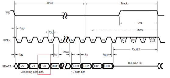
    1、问题描述:我在采用ADC121模数信号转换时会存在数据转换出错(小概率出错),数字信号错误点存在两种现象。一种在前导位Z0位恒高后,后12位数据恒高。另一种在前导位Z0位恒高后,后12位数据恒低。请教一下造成这种现象的具体原因?另外这种积分型的AD芯片,抗干扰能力(空间辐射或传导干扰)如何?

    2、我在电压采样电路原理,实测芯片供电电压3.3V正常,R162采样端输入电压最高220Vdc;电路供电和AD芯片时钟、CS信号电平实测均无异常。AD的模拟量输入存在轻微抖动,但从未超过芯片供电电压。

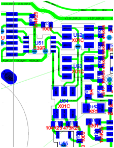
    3、下图对应了此片电路的版图设计,U52、U53、U54为同一原理的三处电压采样,时钟频率8.8MHz,转换速率25ksps,采用轮询模式,三个AD转换芯片共用同一数据总线。

    Thanks

    Yang

  • Hello Cynthia,

    Question:

    1. When I uses ADC121 analog-to-digital signal conversion, there will be data conversion errors (small probability of error), and there are two phenomena in digital signal error points. One type is constant high after the leading bit Z0 bit is constant high, and the last 12 bits are constant high;The other is that after the leading bit Z0 is kept high, the last 12 bits of data are kept low. What are the specific reasons for this phenomenon? May I know How about the anti-interference ability (space radiation or conduction interference) of this integral ADC121 chip?

    2. Please see the principle show, The measured chip power supply voltage is normal at 3.3V, and the R162 sampling terminal input voltage is up to 220Vdc;the circuit power supply and AD chip clock, and CS signal level measured are all normal. The analog input of AD has slight jitter, but it never exceeds the chip supply voltage.

    3. Please see as below for ADC121 design, U52.U53.U54 were three voltage samples of the same principle, the clock frequency was 8.8MHz, the conversion rate was 25ksps, the polling mode was adopted, and the three AD conversion chips were share the same data line.

    I'm looking forward for your reply,thanks!

    Best regards.

    Yang

  • Yang,

    This is interesting. If I understand correctly, the device will output all highs, or all lows, regardless of the ADC input?

    Have you been able to get out correct output data form the device at all?  Or does this happen randomly? at specific input voltages?

    The leading zero bits should all be low, there should not be a time where any of the leading Zero bits are high. Are you seeing the Zero bits high?