This thread has been locked.

If you have a related question, please click the "Ask a related question" button in the top right corner. The newly created question will be automatically linked to this question.

ADS122C04: Minimum RESET Time

Part Number: ADS122C04
Other Parts Discussed in Thread: ADS122U04

Folks,

We have implemented the ADS122C04.   Power to both AVDD and DVDD are stable for minutes.    We pulse the reset pin and ~4us after the rising edge we start writing to the I2C bus.

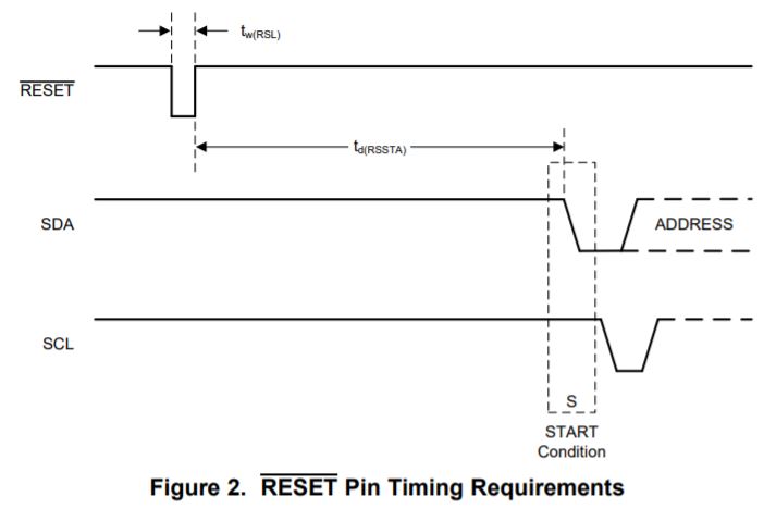
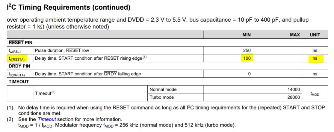
Per the datasheet this should work:


But we're getting NACK's when writing to the register pointer.    For example, here is an example scope shot writing to device address 0x40h (7-bit addressing) and register 0x40h (WREG).

Zooming in a little we see the following:

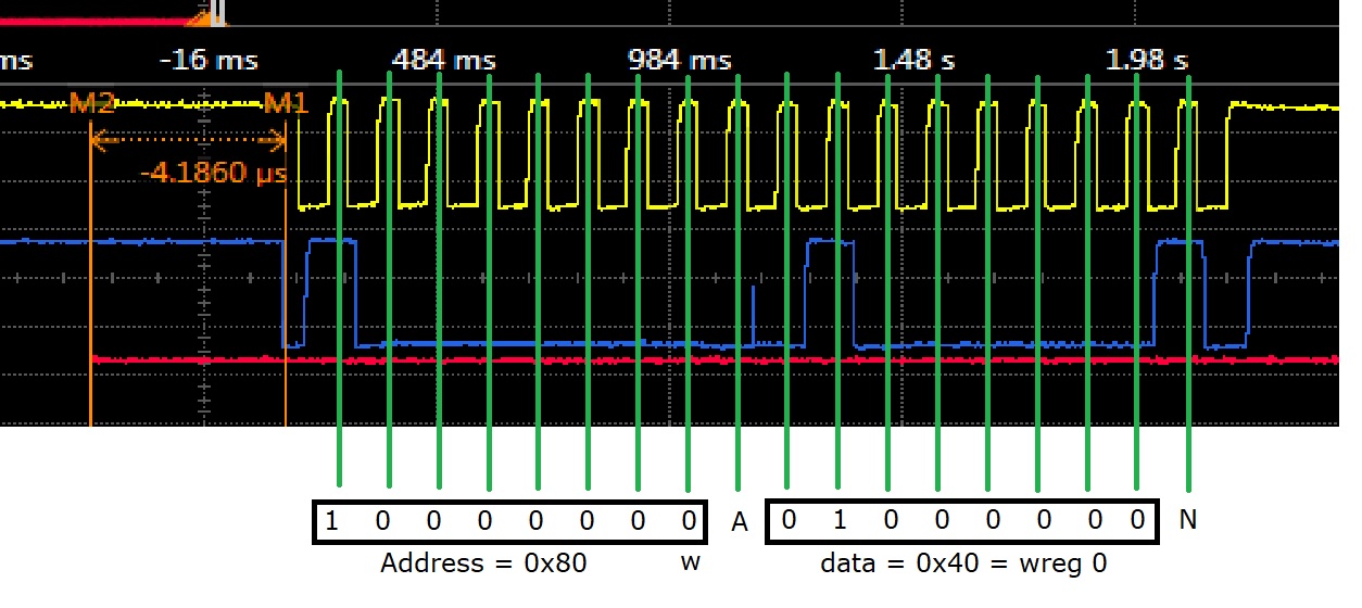
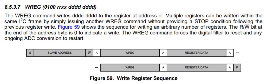
This matches section 8.5.3.7 of the datasheet:


Increasing the time wait time to >25us, seems to solve this problem.

We suspect that the required delay is closer to the TIMEOUT period as specified in the datasheet.    In the case of normal clock mode (256kHz), this would be 14000 x (1/256kHz) ~= 54.7us.    We also suspect that the datasheet may have a typo; spec'ing td(RSSTA) in ns as opposed to the correct us.

Looking forward to a little clarification on this subject.

Don 

  • Hi Don,

    Could you attach the scope picture as a file attachment?  It is difficult to get good resolution from the forum picture in the post.  We see that when the device is addressed there is a proper ACK, so the device is communicating up to that point.  However when the next byte is transferred there is an error and a NACK is issued.  This requires the timeout for the communication that was in error to clear.  So it doesn't appear that the timing after the RESET pin goes high is the issue.

    It is a little difficult to tell, but it would appear that Fast+ mode is being used.  What resistance values are being used for the pullups?  And where are the scope probes being placed?  It would be good to establish a scope shot of the communication at or as close as possible to the ADS122C04 device pins to make sure there are no delays due to bus capacitance.

    Have you tried other commands to see if they are working or has just the WREG been called?  Also, is there any difference if the SCL clock frequency is reduced?  

    Best regards,

    Bob B

  • Hi Bob,

    Confirmed, we are using a 1MHz I2C clock, thus fast mode plus.   When we slow the clock down to ~200kHz, the problem seems to go away, though candidly, I suspect, this pushes the second byte N/ACK beyond the suspected 50us window.  

    Scope shot attached.   This is the highest resolution that I have.   Will confirm where scope probe placement is on Monday.   

    I'm looking into what the pull-up resistor values are, though I've referenced this app-note as a good tool to calculate them:

    https://www.ti.com/lit/an/slva689/slva689.pdf

    Would you please explain what you meant by this:

    ----

    This requires the timeout for the communication that was in error to clear.  So it doesn't appear that the timing after the RESET pin goes high is the issue.

    ----

    Don

  • Hi Don,

    I apologize for the delayed response.  There are two considerations.  The first one is the start of communication following the rising edge of the RESET pin.  This is shown as 100ns in the datasheet as you pointed out at the original post.  The second consideration is not clearly specified and that is the timing as to when you can reconfigure the ADS122C04 following the RESET pin going high. This actually differs from start of communication.

    Note that the ADS122C04 is ACKing and recognizing that communication has started to the ADS122C04.

    This demonstrates that communication is possible at this point.  However, although the communication is possible it does not mean that the device is ready to be configured.  Unfortunately I cannot find specific design information regarding this timing and will have to attempt to contact the designer for additional information.  Most likely we will need to update the datasheet with additional timing information.  It would appear that the timing from the RESET pin going high to start of communication for a device configuration is only valid when using Standard mode timing.  I will respond again when I receive a clarification.

    The ADS122U04, although using a different interface, is very similar in operation to the ADS122C04.  The ADS122U04 timing requires a minimum delay of 80us.  Based on your your 200kHz timing experiment the delay time appears to be similar.  The device decode for the command takes place on the bit 7 of the 8 bit command.  This would occur approximately on the 16th clock from the beginning of communication or approximately 80us from the first clock.

    I believe that by delaying the initial delay from 4us to 84us should be sufficient for operating in Fast Plus mode.  I calculated from 200kHz period (5us) times 16 clocks plus 4us initial delay which equals 84us which appears to be working. You could increase this slightly if you want a little guard band.

    Best regards,

    Bob B

  • Thanks Bob,

    Please do let me know what the IC designers come back with.

    Don

  • Hi Don,

    This can become a complicated answer.  The designer says that if the NACK is ignored that the register write would still take place.  So the communication does work, just not as expected.  Essentially it takes 80us from the rising edge of the RESET pin until all of the internal trim information is read from the device.  During this time communication is possible, but there is a hold on the ACK signal for commands until this update period ends.

    So to get an ACK on the command, you would need to make sure that 80us has passed prior to the ACK signal time frame.  This is the same delay required for the ADS122U04, so my theory was correct that I posted previously.

    We need 80us delay prior to the WREG decode.  We are using 1MHz clock for SCL, and each clock period would be 1us.  After 16 clock periods (16us) the WREG command will decode. 80us - 16us = 64us, so you would require at least 64us delay to meet the 80us total time to receive the WREG ACK.  This is assuming perfect timing and no clock drift.

    The 80us is based on all process corners and operating temperatures.  So it could be possible that a shorter time delay would work on some devices at room temperature, but 80us is the safe time and should be the time used for calculation to ensure the ACK.

    Best regards,

    Bob B

  • Thanks Bob,

    We're adding an 80us startup delay time until we get a firm number.

    Don