This thread has been locked.

If you have a related question, please click the "Ask a related question" button in the top right corner. The newly created question will be automatically linked to this question.

DAC101C081: I2C communication question

Part Number: DAC101C081

HI,

I have problem communicating with the DAC. ADR0 is connected to ground and im using chip address 0001101.

the communication is speeding at 100KHz, and signals / timing seems to be matching as per spec, but the DAC output stays to 0...

Question, should the DAC be sending a NAK SDA to 1 if the chip address is not the good one? because whatever the address im sending to it at the moment, the DAC returns ACK, SDA to 0. I did swap the part in case... same issue.

Thanks for your support!

  • Hi Pasca,

    Have you confirmed this with an oscilloscope? Could the SDA pin just be held low all the time? Can you share your schematic?

    The device should only acknowledge it's address or the broadcast address.

  • Hi Paul,

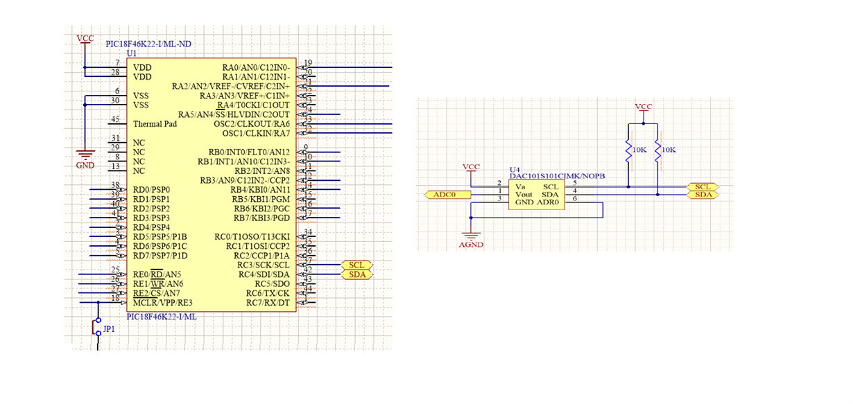
    Thanks for quick reply. The schematic of the I2C portion is pretty simple, see below: Note for some privacy reasons, I kept only the I2C portion of the circuitry here.

    I tried reducing the pull up resistors value and still he same issue

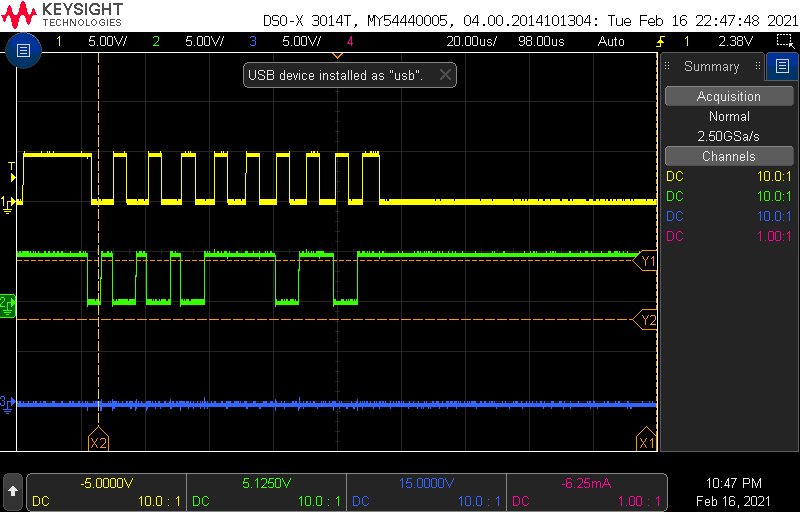
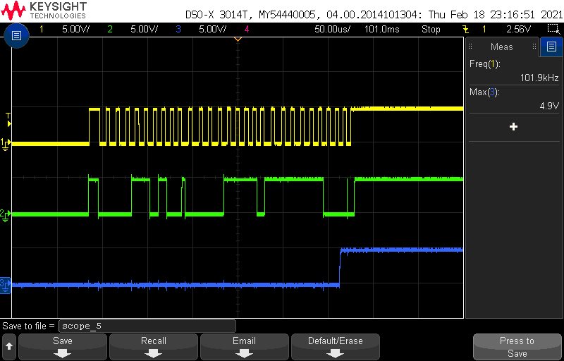
    The scope reading is showed below: Yellow is the SCL, green SDA and blue DAC output.

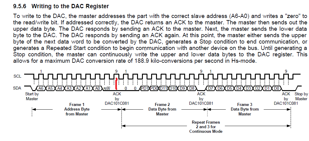
    Following the write sequence as show in the spec sheet, I was expecting the SDA to be driven low by the DAC to ACK the chip address and write command, note that in my code, I'm releasing SDA pin right after writing the write bit to 0

    Any comment, guidelines will be appreciated,

    Thanks for your support!

  • Weird for some reasons, images didnt follow.

    Paul, can you use the email link to my account to follow up on this, its my work email.

    Thanks,

  • Hi Pasca, when posting image, you must use the "insert media" button on the menu.  Simply pasting images does not work.  

    Please try attaching the images again.  If you have issues, we can move to email.  Thanks,

    Paul

  • take 2 :)

    Hi Paul,

    Thanks for quick reply. The schematic of the I2C portion is pretty simple, see below: Note for some privacy reasons, I kept only the I2C portion of the circuitry here.

    I tried reducing the pull up resistors value and still he same issue.

    The scope reading is showed below: Yellow is the SCL, green SDA and blue DAC output.


    Following the write sequence as show in the spec sheet, I was expecting the SDA to be driven low by the DAC to ACK the chip address and write command, note that in my code, I'm releasing SDA pin right after writing the write bit to 0

    Any comment, guidelines will be appreciated,

    Thanks for your support!

  • Hi Pasca,

    It looks like you are using the correct address. Is your communication meeting the timing requirements for standard mode?

    It is important that the setup and hold times are being met. From your scope shot it looks like your data values are changing very close to the clock rising edge at some points, but it may be that the scope time scale is too large for me to see. 

    In addition, are the DAC AGND and PIC GND shared somewhere else in your schematic?

  • Hi,

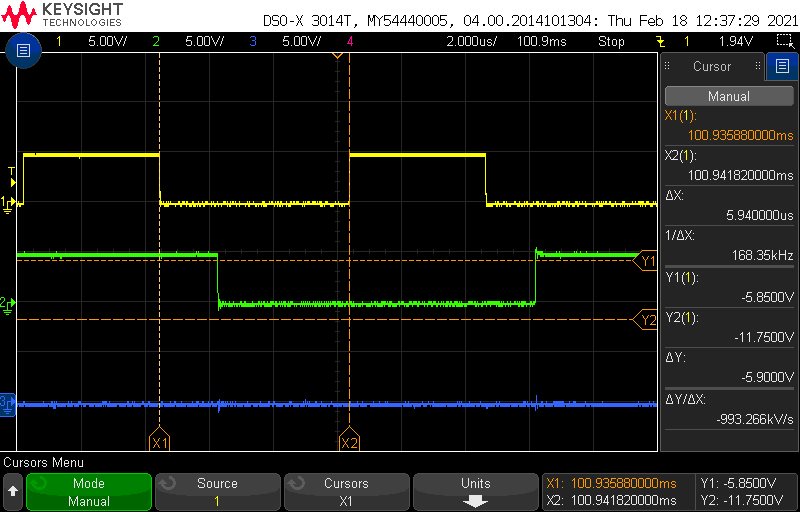
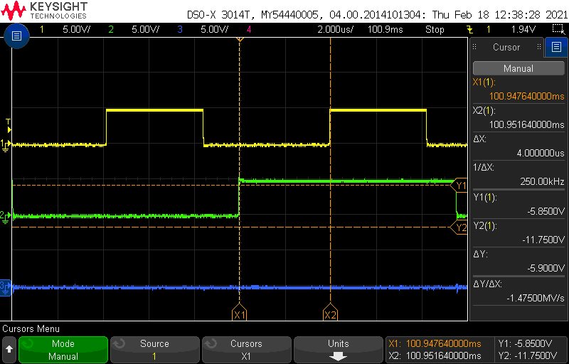
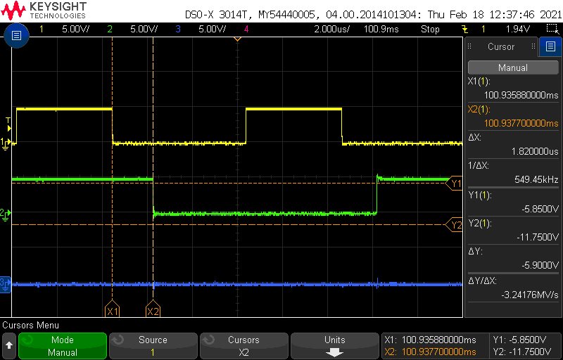
    See timing below, to me everything looks fine. Im running a little lower then 100KHz (95KHZ) but that should not be problematic?

    tLOW

    tHIGH

    Data setup time:

    Data Hold time:

    My understanding is that everything looks fine, Ill wait to get your comments.

    The AGND is only separated by GDN by a 0 ohm resistor, the goal is to differentiate them for making sure we pay attention to AGND during routing.

    Thanks,

  • As a different line of pursuit, perhaps you have an unused PWM output that could be used instead of a DAC. The following observations prompted me to consider this:

    1. The DAC reference is the same as the MCU supply voltage.

    2. The resolution is only 10 bits, and the update rate is limited by the I2C speeds to the order of kHz.

    3. The CPU clock is presumed to be 12MHz, although this may well not be the case (or the MCU may be asleep, etc).

    PWM will likely have linearity at least as good as the DAC, and given a 12MHz clock would have similar update rate to that of the DAC, with less software overhead. On the other hand, it needs an RC filter and a buffer. If the voltage is used to drive loads with inherent "inertia", the RC filter and buffer may turn out not to be necessary.

    I'm not suggesting to just drop the DAC - it may be the best fit there's for your application, but I did want to share at least one alternative.

    Another observation - and this is very broad and general, as we of course don't know the specifics of your application: the 0R "AGND to DGND" link may perform even worse than the "willy nilly" routing it's supposed to avoid, since it adds bulk inductance. All high frequency return currents from the analog domain to the MCU will flow through it and automatically couple into all loads, since there's now a common series circuit element between all digital signal loads in the analog domain and their source (the MCU). At the very least you'd want to configure minimum viable drive strength on the MCU pins that drive signals into the analog domain (SCL, SDA, etc). On fairly recent Altium, IIRC there's a way of defining a net join area on the PCB, without resorting to links. Adding an actual physical part to enforce a manual routing rule seems a workaround to a fundamental problem of not having a layout review: it'd presumably catch such things. When doing the layout, the net names ought to be secondary to a well-performing layout stemming from following the function of the circuitry being laid out :) There's often some leeway in routing, in that not all of the AGND is equally susceptible to "digital noise". The foregoing is, again, very general and may not apply at all to your circumstances.

  • Hi Pasca,

    Kuba has brought up some good points for you to consider. 

    I'll continue to help debug your I2C communication. Thank you for providing the timing scope shots. They do look correct. The schematic symbol from an earlier screenshot you provided looks correct for the 6-Lead SOT package pinout, can you verify that the footprint you used matches as well? Also verify that the SDA and SCL signals are reaching the DAC pins, as well as verify the voltages on the supply, ground, and ADR0 pin. It's possible one of these pins does not have a good connection. 

  • Hi Katlynne,

    All your validation proposal have been already looked at and tripple confirmed :) I was pretty confident about my firmware and the timing, your confirmation on proper timing forced me to swap the chip for a third time… luckily this time it was the good one. Everything is now working, I will have to talk with our SMT rework person to close this by understanding what he might have done wrong while reworking the IC.


    Thanks to you and your team for your great support and please say big thanks to Kuba for his proposal.

  • Hi Pasca,

    Great to hear you got it working. Please let us know if there's anything else we can do for you!