This thread has been locked.

If you have a related question, please click the "Ask a related question" button in the top right corner. The newly created question will be automatically linked to this question.

ADS4126: The ADS4126 provides a CMOS interface and an LVDS interface, which is lower power?

Part Number: ADS4126


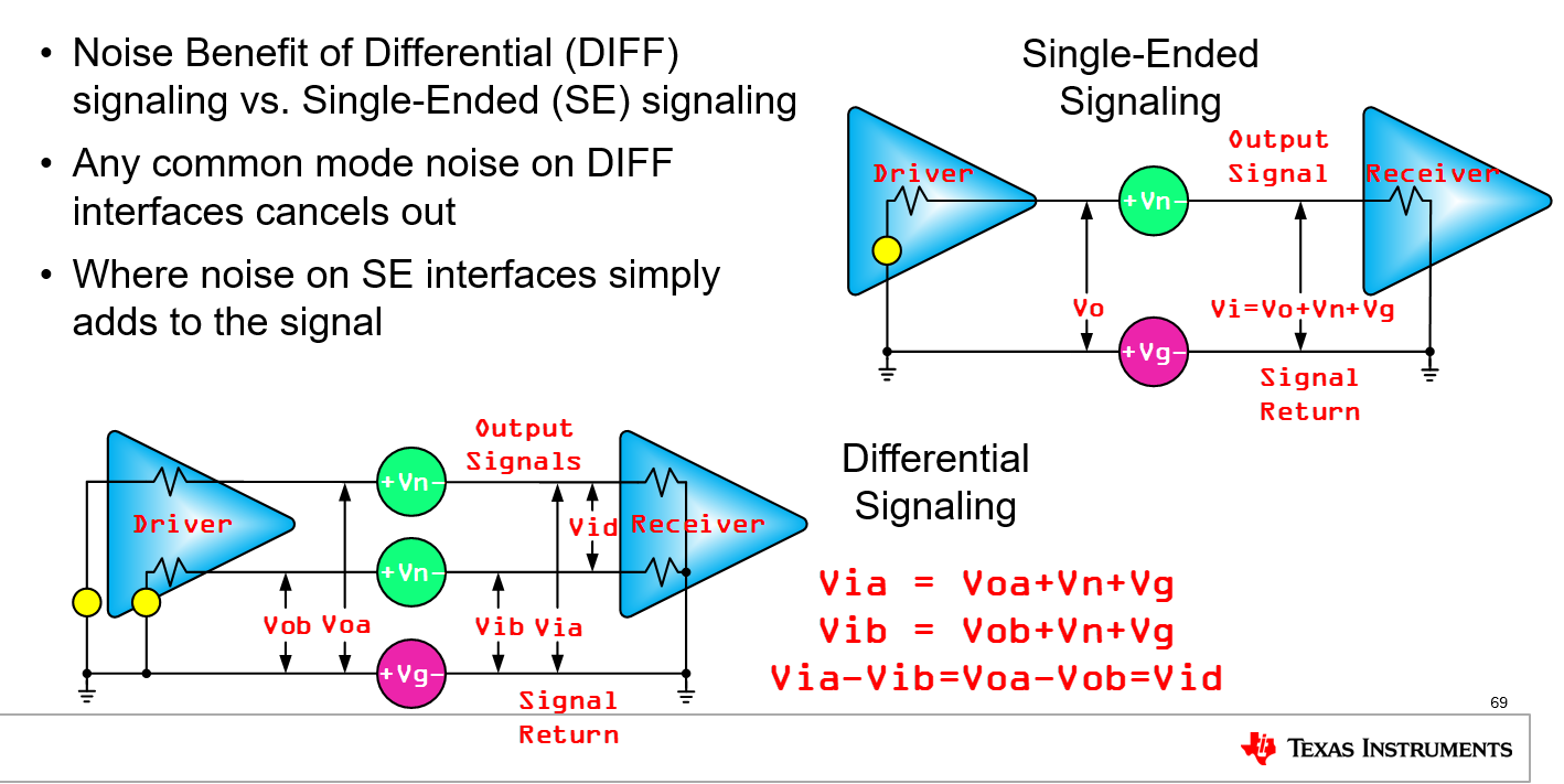
The LVDS is a differential standard while the CMOS is a single ended standard.

Are both I/O standards useable for the full range of sampling rate permitted by this device?

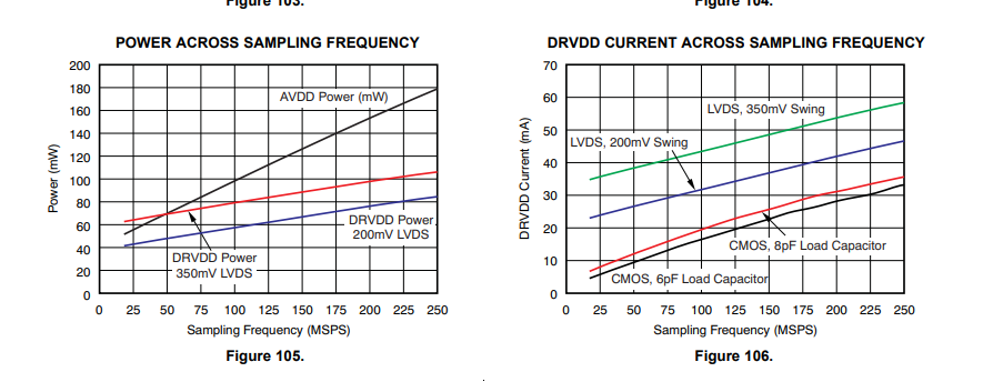
Which of these is expected to give lower power dissipation for a given data rate?

Since the ADC will be quite close to the FPGA or ASIC accessing it anyway, what is the benefit of having LVDS which just doubles the required pin count for connection to this ADC?

The datasheet page 7 shows power dissipation for use of LVDS and CMOS interface. From this, it implies that use of CMOS is lower power than LVDS. However, it is not clear if this is the case for full range of sampling rate of this ADC. 

  • Hi Hassan,

    What is the sample rate that you plan to use for this ADC? This will be a good starting point.

    Typically, 100MSPS and lower will give you a better power savings when using CMOS, beyond that, the LVDS is a constant power regardless of sample rate.

    Hope that helps.

    Regards,

    Rob

  • ok, as far as I am aware, our target is 120MSPS. What would be a power efficient interface for this? i.e how do I determine the power dissipation figures for CMOS vs LVDS for this?

    As long as the power dissipation here in the interface is actually quite small compared with the rest of the system, it may not be a big deal. However, since this interface is running at a quite a high speed, I believe that we need to look at the interface power dissipation a bit closely.

  • Hi Hassan,

    If you have an EVM or your own system board. You could look at the 1.8V DRVDD supply current only, this would give you the difference in power between these two interfaces.

    If you are requesting us to do this on the bench with our EVM please let me know.

    Regards,

    Rob

  • Hi Hassan,

    I found this plot in the datasheet on page 51.

    For this converter design, it looks like CMOS would be the way to go in order to keep the power as low as possible.

    Regards,

    Rob

  • Thanks, this has almost clarified my doubts and confirmed my suspicion. 

    I am curious to know why we have LVDS interface on this device. We are not going to use it at 100sMHz or GHz range and the ADC will be on the same PCB as the FPGA or ASIC. Why even bother including an LVDS interface? It does not make sense at all.

  • Hi Hassan,

    There are two immediate reasons why someone would use LVDS over a CMOS digital interface.

    1) LVDS, offers higher common mode rejection to noise. Since these signals are differential, the inherent noise immunity goes up over a single-end CMOS connection.

    2) another reason, is that LVDS, is constant current, hence the power which is a disadvantage, but the down side is noise again for CMOS interfaces, when you have many single-ended transitions all happening at once, this can cause for a lot of current to be "dumped" onto the ground plane, this typically happens as the zero transition when the outputs go from all 000000's to all 11111's. This in effect, causes noise, which can typically translate into EMI issues, and/or offset of the ADC being higher than normal. A way around this is to provide a series resistor on each output of the digital CMOS output.

    I attached a slide to help go through the calculations.

    Hope this helps.

    Regards,

    Rob

  • Thanks for this buddy.

    Basically, if the ADC is designed to correctly operate at high frequency upto its limit, with the CMOS interface, and the PCB design is done in a sensible way to account for signal integrity, why would one really need to use LVDS?

    LVDS uses double amount of pins which means the FPGA/ASIC must have more pins and the PCB layout must do more work.

    I can see that SSN can be a problem with multiple outputs switching roughly at the same time. However, I assume that the TI designer of the ADC will have done the design in such a way that the SSN should not cause data corruption across the operating range of the device. If the ADC is on the same PCB as the FPGA and directly connected to it via PCB tracks, I see no advantage of using LVDS over CMOS. Yes, across a backplane or over longer distances it may certainly makes sense. If the ADC is so close to the FPGA/ASIC then the noise immunity from LVDS cannot benefit much as long as the PCB design is done with signal and power integrity kept in kind.

    Unless the ADC is intended to be communicated across long distance via back plane or cables, I do not see any reason for opting for LVDS as the noise immunity issue can be mitigated with sensible PCB design in the first place. Is my understanding wrong?

  • Hi Hassan,

    Your understanding is correct.

    However, I would definitely use, or at the very least, put a placeholder for a series resistor in-between each digital output of the ADC and input of the FPGA/ASIC. The resistor should be located closer to the ADC's outputs. I have found in many cases this is needed, even if the distance is short.

    Regards,

    Rob

  • Could you kindly describe one specific case where we prefer LVDS over CMOS inspite of it needing double number of pins and not being all that better than CMOS in the scenarios where we would use this ADC. It will help me understand such parts in the future in a better way.

    Thanks.

  • Hi Hassan,

    I think some of the examples were described in the previous posts. But I will try to summarize, who one would use LVDS vs. CMOS

    Regards,

    Rob

    •Single-Ended Outputs (CMOS)
    –More common output logic standard interface, also cheap
    –Limited speed capabilities due to board parasitics and output loading
    –More noise due to larger signal swing (5/3.3/3/1.8V) causing digital ground bounce
    –Series termination resistor for each bit recommended
    •Differential Outputs (LVDS/CML)
    –More popular because data rates are increasing
    –Significantly faster than single-ended CMOS
    –Less noise due to common-mode rejection and small signal swing (320m/200mVpp differential)
    –Differential resistor termination required (may or may not be included in FPGA)
    –Twice the number of traces routes and FPGA pins required
    –Simpler data captures compared to single-ended CMOS demuxed solutions