This thread has been locked.

If you have a related question, please click the "Ask a related question" button in the top right corner. The newly created question will be automatically linked to this question.

ADS7263: Request to understand larger than expected ADC offset voltages (0.08 volts)

Part Number: ADS7263

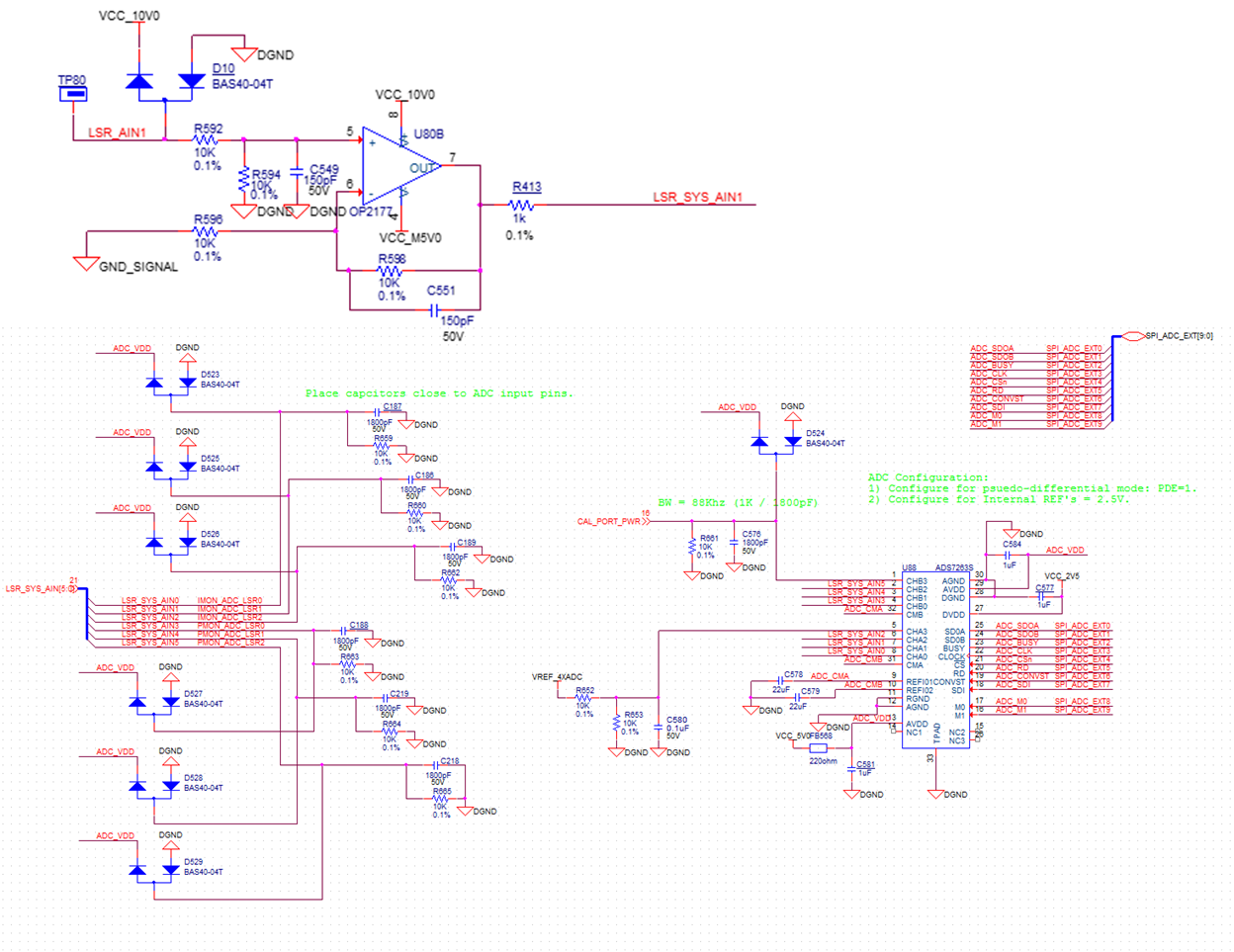
For my application, I have an ADS7263 configured for 8 single ended 0-5V input channels. To use the ADC in single ended mode, the REF outputs (set for 2.5V) are connected to the CMA and CMB inputs. The sample rate is 250K samples per second. The good news is that the basic functionality seems to work as intended. The only issue is that there is a large analog offset of about 0.08 volts on each of the input channels when the actual value is 0 volts. The ADC value for an input of 2.49 volts matches the expected value (half scale) almost perfectly - within 0.1%. I have verified the supply voltages (5.0V for AVDD and 2.5V for DVDD) as well as the value of the references and common mode inputs (very close to 2.4999 volts). While the apparent error / offset for 0 volt input is not huge with respect to full scale (about 1%), I was expecting the error to be much smaller. Please take a look and let me know if you can help me sort out what is causing the large offset voltage.

  • Hi Randy,

    Thank you for your post.

    How do you have the REFCM register configured? It looks like you are making an external connection between REFIOx and the CMx input pins. This is perfectly ok, (although I noticed you have ADC_CMA connected to the CMB input pin and vice versa), but I wonder if using the internal connection makes any difference. For example, you could try writing REFCM = 0xFFF0. For all CHBx measurements, ADC B will use REFIO2 as the CMB common-mode source and as the internal reference voltage. Similarly, for all CHAx measurements, ADC A will use REFIO1 as the CMA common-mode source and as the internal reference voltage.

    Actually, since you have configured both REFIOx pins to be 2.5 V, there is no reason not to use the same REFIO voltage for both ADCs. REFCM could be set to 0xFF00 in that case, and REFIO2 can be powered down by setting REFDAC2 = 0x07FF. 

    If this does not improve the offset, could you share more details about the error? Is it both ADCs and all input selections (i.e. CHA0-CHA3)? If you externally short the channel input pin with corresponding REFIOx pin (assuming you keep the external connection from REFIOx to CMx), does the offset disappear?

    Best regards,

  • Hi Ryan,

    Thank you for the detailed response. Here is some more information on the current configuration 

    Register Load Sequence:

    UPDATE_CONFIG_REG x"1060";
    UPDATE_REFDAC1_NEXT x"1002";
    UPDATE_REFDAC1_REG x"03FF";
    UPDATE_REFDAC2_NEXT x"1005";
    UPDATE_REFDAC2_REG x"03FF";
    UPDATE_REFDCM_NEXT x"100C";
    UPDATE_REFCM_REG x"00F0";

    Measurement Data:

    I have verified that 3 of the four inputs on both A and B channels have the same offset error at 0 volts input. The count values were measured from 0x0434 to 0x0480 for input voltages close to 0 volts (actual inputs were 0.025 volts). One input has a 2.492 volt input driven from an external independent reference voltage - the count value was 0x7FBC which is within a small fraction of a percent error. 

    Anyway, I will be trying out the internal reference configuration as you mention and let you know if that changes the behavior. 

  • Update,

    Changing to internal references (change REFCM to xFFF0) did not appear to change anything. When I tried powering down REFDAC2 (REFCM=xFF00 and REFDAC2=x07FF), the B side ADC's worked same as before, but the A-side channels were all shifted by 0x7FFF.

  • Hi Randy,

    Thank you for verifying that the internal reference change didn't make a difference.  Do you see a similar ~80mV offset when you try putting 5V (full scale) on the inputs?  Can you also try a couple channels with the input shorted directly at the pin to ground and let us know what you see?

  • Hi Tom,

    Here are some more notes from today's testing.

    • The inputs all driven by OpAmps but go through a resistor divider with an RC network at each ADC input. The resistor in series with the OpAmp output is 1K ohm. Each ADC input measures about 0.025 volts DC in this condition while the OpAmp side is very close to 0.000 volts. It appears that there is 25uA of leakage current coming out of the ADC input which is way higher than the 16nA I was expecting from the data sheet.
    • In this configuration, the count value is about 0x0440 which would should map to a voltage of 0.083 mvolts. 
    • When I short out one of the inputs so that the 0.025 volts gets nulled out, the ADC count value is 0x005C which would map to a voltage of 0.007 volts.
    • When I apply 4.976 volts to one of the inputs, the count value is 0xFFF4. If the input voltage goes any higher, the count value will max out at 0xFFFC.

    So, one new question is why the ADC input leakage current is so much higher than expected? My guess is that this ADC is expecting to be driven directly from an OpAmp output rather than through the RC network I am using. Please confirm if this is the case.

  • Hi Randy,

    Thanks for the added detail!  The ADS7263 is a succesive approximation register (SAR) type ADC.  These SAR type devices often rest the internal sample and hold switch to a known voltage after the conversion process is complete (VREF for example), so that in the next conversion cycle, they start from a known voltage stored on the internal sample and hold cap.  The ability of the internal sample and hold cap to charge to within 1/2 LSB (ideally) of the new sample depends on the input impedance and the drive capability of whatever amplifier might be attached to the input.  Here is a series of informative videos to help explain a little about the nuiances of driving a SAR converter.

    With the input directly shorted to ground at the pin, I actually suspected you would see a smaller code deviation than what you did see - 0x005C is still larger than what I would expect, so you may have some layout/grounding issues.  What op amps are you using to drive the inputs?  If you extend the sampling time by reducing the 250kSPS throughput to say 125kSPS (for debug purposes), does the offset change?

  • I think the OpAmp itself is not the issue so much as the RC network between OpAmp output and ADC input. There is a 1K resistor from OpAmp output to ADC Input. The ADC Input then has another 10K resistor and an 1800pF capacitor to ground. I was counting on the capacitor to provide a low AC impedance for the ADC input sample and hold circuit. I may end up just adding another set of OpAmp buffers to drive the ADC inputs.

  • Depending on the speed of your SCLK and the bandwidth of your amplifier, you may be right!  If you can provide those details, we'll take a closer look!  Adding another amplifier stage may not be necessary and could lead to additional error, so do let us know what you are comfortable sharing here on the open forum.  

  • Hi Tom,

    Attached is a bit map that shows the schematic sheet with the ADS7263 along with an example of one of the OpAmp circuits that provides one of the analog signals of interest. It may be sufficient to simply reduce the series resistor from 1K to something like 100 ohms to get a much more accurate ADC acquisition. Please let me know if you have other ideas that you think might work better.    

  • Hi Randy,

    What is your clock speed?  This will determine your acquisition time which will impact the BW needs of the amplifier and choice of R/C ahead of AINx.

  • The two ADC's are running at 1Meg sample/sec. However, we are 4x muxing each of the two ADC's so that each of the 8 total ADC channels operate at 250K samples/sec. The analog channels ahead of the ADC's are intended to have about 100Khz of bandwidth.

  • Hi Randy,

    OK, thanks for the additional info.  Since you are running the parts full speed, you are going to need a faster opamp to most likely.  If you are happy with your current configuration and just want to add a buffer, that might be an option for you.  If you went through the "Introduction to SAR ADC Front-End Component Selection" video, there was a description of the Analog Engineer's Calculator tool.  That tool contains a SAR ADC Drive calculator that helps pick ballpark Rfilt and Cfilt values and also provide guidance on the BW of the amplifier needed to drive the ADC input.  From the specs in the ADS7263 datasheet you have 100nS of acquisition time to fully settle the ADC input.  With a 45pF S/H cap at 14-bit resolution, the SAR Drive calulator shows an amplifier with ~43MHz GBW is needed to fully settle the input.

  • Thanks for the additional information. I think I have enough to sort out the best solution for my application.