This thread has been locked.

If you have a related question, please click the "Ask a related question" button in the top right corner. The newly created question will be automatically linked to this question.

DAC7822: OFFSET AT THE VOLTAGE OUTPUT

Part Number: DAC7822
Other Parts Discussed in Thread: OPA2822, OPA828, OPA2228

Dear alI,

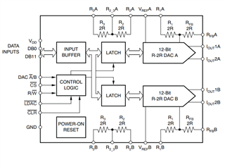
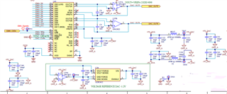
I have a design using DAC7822 working as a positive voltage output. Please find attached the schematic.

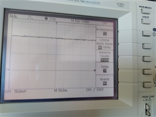
On the output for a "code 0" I have an offset of 200mV, see scope image below.

I need to have offset=0V for code 0,. Is there any way to to get it? What changes should I do to get it? Should I replace the output amplifier? What reference do toy recomenende me?

Power supplies (+5V_DAC and  -5V_DAC) and reference voltage (-1V2) are clean and stables.

Thanks in advance,

Joaquín.

  • Hi Joaquin,

    Is this offset consistent across all codes? For example, you output should ideally be 0V to 1.2V, correct? Is it currently 0.2V to 1.4V, or is it 0.2V to 1.2V and the lower codes make no impact on the output?

    The bias current of the OPA2822 is a bit high, so I would expect some offset, but not 200mV.  Can you measure the voltage on U37 pin 2 or pin 6? It should be 0V.  

  • Hi Paul,

    Thank you for your support.

    Sorry for the delay answer but the person in charge of developing the software of this systems was not available last days and I couldnt do the test until now.

    The offset is consistent on all values. For Code 0, the output is 0.1857mV, for code=2048 output= 1,385 mV and for code=4096 output= 2,585mV.

    For low values, for example, code=5 output= 0.187mV, for code=10 output=0,192mV.

    Voltage on pin 2, U37, is 0.000V.

    One more thing is that the output goes to 0 to 2.4V (+Offset)  when it should only go 0 to 1.2V because the reference is -1.2V. I have revised the datasheet but I dont see why is this. Any idea?

    Thanks in advance,

    Joaquin.

  • Hi Joaquin,

    The gain is approximately 2x what you want because you are only using the RFB pin. Note that the total impedance of R2R ladder at full-scale would be R, and the value of the RFB and R1 resistors is 2×R..  So you gain for you inverting amplifier would be -2R/R, or -2x.  If you want -1x, you need to short R1 and RFB they are in parallel.

    I think your offset is caused by the OPA2822's input bias current.  This would be current flowing into the input of the opamp.  On an ideal op amp this is zero, but for a real op amp, it can vary.  The OPA2822 is specified for 9µA typical, and 18µA max@25°C. The offset voltage is a bit better, at 1.2mV.

    This means that the virtual ground at the inverting input node would be within that voltage, assuming the amp is in its linear operating range.  The value of RFB is typically 20kΩ.  Now we know that that bias current would be flowing through the feedback path, so you would have an undesired offset of 20kΩ×9µA, or 180mV.  Now taking into account that we are dealing with typical values, I think this explains the 185mV offset.

    So you need to short R1 and RFB together and select a different amplifier with lower bias current, maybe a device like the OPA828.

    Thanks!

    Paul

  • Hi Paul,

    Thank you very much for your explanations. Everything clear now.

    Before close this thread, just one more question. As I need to make the actual board functional, I need a direct replacement for OPA2822 (dual OA) so looking for a new part, I have found OPA2228, which it has an Ibias= 2.5nA and BW=33MHZ, which I think is ok for us. Do you see any detail for this part not acceptable for this application?

    Thanks in advance,

    Joaquin.

  • Hi,

    OPA2228 is good choice with its 10nA Max Bias current which will result in 20K * 10nA = 200uV offset and its input offset voltage is very low ( max 200uV)

    Regards,

    AK

  • Ok, thank you very much.

    Great support!

    Regards,

    Joaquin