This thread has been locked.

If you have a related question, please click the "Ask a related question" button in the top right corner. The newly created question will be automatically linked to this question.

ADS131E06: ADS131E06: Error during default register read through SPI interface

Part Number: ADS131E06
Other Parts Discussed in Thread: ADS124S08

Hi,

I'm trying to read Register address 0x00 through SPI. I'm continuously reading register address @ 0x00 after making ADC's RESET line HIGH. I noticed that MISO data changes during each read cycle. It reads random data. Default register value is 0xD2 @ 0x00.

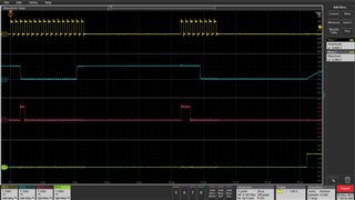
Oscilloscope captures attached for ADS131E06.

Yellow: SPI CLK 
Blue: MISO
RED: MOSI
Green: CS


Let me know if you have a clue to debug this error

  • Hello Sadashiva,

    Thank you for your post.

    The command to read the ID Register is 0x20 0x00. Following the RREG command, you should send a null byte (0x00) while keeping /CS low. The contents of the ID register will be output on DOUT as you send the NULL byte. It appears that you are sending 0xC0 on MOSI in the third byte.

    The correct default value for ADS131E06 is 0xD1.

    Are you following the POR sequence correctly? One test would be to leave the power supplies on, manually pulse the /RESET pin, and read the ID register again. If it reads correctly, this would indicate that your initial POR sequence was not following the data sheet timing guidelines.

    Best regards,

    Ryan

  • Hi Sadashiva,

    Apologies for accidentally deleting both of your replies - I just meant to delete the duplicate post. Slight smile 

    Here was your original reply:

    "Thanks Ryan,

    I hope you have seen oscilloscope captures which was attached in initial query. I'm sending 2 bytes (0x20 0x00) from MOSI while keeping CS low. Manually pule of RESET line also already taken care. What is POR sequence requirement for ADS131E06 apart from Figure. 65? "Figure 65. Power-Up Timing Diagram" is taken care"

  • Hi Sadashiva,

    The RREG command requires 3 total bytes: 2 bytes for the command op-code, and a third byte to read the ADC response. Therefore you must send 0x20 0x00 0x00. In your scope capture, you are sending 0x20 0x00 0xC0. While you are sending 0xC0 in your third byte, the MISO pin is outputting 0xF0, which is not a valid ID register value.

    Is /CS transitioning from high to low before you send the RREG command? It would be helpful to see the beginning and end of the frame to validate the proper communication protocol.

    Figure 65 is all that is required to complete the POR. This figure assumes that you have waited 2^18*tCLK or tBG (VCAP > 1.1 V), whichever is longer. To verify that this is not the cause of the problem, please issue an extra reset pulse to the ADC while power supplies remain ON and check the ID register again.

  • Ryan,

    On MOSI line, 2nd byte is 0x00 so, SPI controller responded with third byte, the MISO pin is outputting 0xF0. Typically SPI controller  will ignore extra byte (3rd byte in this case) on MOSI line i.e., 0xC0. 

    Having said that, I looked at firmware code. 3rd byte, 0xC0 is not sent across MOSI line in controller's code. Yet to find root cause of 0xC0 as a 3rd byte on MOSI line. Looks strange from firmware perspective.

    Same firmware code is working fine for ADS124S08. Both these ADCs (ADS131E06 & ADS124S08) shares same SPI bus with different chip selects lines.

    I will update on this soon...

    // -------controller's firmware -----------

    // 1. Bring Slave Select LOW

    HAL_GPIO_WritePin(CS_SPI_ADC_AK_GPIO_Port, CS_SPI_ADC_AK_Pin, GPIO_PIN_RESET);
    HAL_Delay(10);

    // 2. Transmit register + 0x20 (to set bit to high, read mode)
    spiTxBuf[0]=spiAddr|0x20;
    spiTxBuf[1]=0x00;
    HAL_SPI_Transmit(&hspi3, spiTxBuf, 2, 50);

    // 3. Receive data
    HAL_SPI_Receive(&hspi3, spiRxBuf, bytesNumber, 50);

    // 4. Bring slave select HIGH
    HAL_GPIO_WritePin(CS_SPI_ADC_AK_GPIO_Port, CS_SPI_ADC_AK_Pin, GPIO_PIN_SET);