Hi guys,
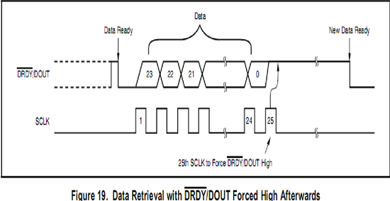
I'm working on my school project and I was wondering if I can get some help with my SPI code for the ADS1231? Im using the MSP430BT5190 microcontroller(the one included in EZ430 RF2560). The way the ADS1231 works is that it will pull its DRDY line low when it is ready to start shifting out data and it is at this time the serial clock is started. When 24 bits are shifted out, the DRDY goes back to high and, from my understanding, the Serial Clock stops. I have a diagram of how I plan on connecting the pins on my microcontroller to the ADS below as well. I plan on connecting both p3.0 and p3.2 to the DRDY/DATAOUT and the P3.3 to the SCLK. P3.0 will handle the DRDY signal and P3.2 will handle the SOMI. Anyway, I was wondering about a few details.
With the code that I have below, am I correctly stopping and starting the Serial clock? The Serial clocks should only be applied when DRDY is low so I did this by stating if(!P3IN). It will turn on again when DRDY is high so if(P3IN). I stopped and started the SCLK by doing: UCB0CTL1 &= ~UCSWRST;
Secondly, isn't there some conversion that I need to do so that the data that I'm getting is standardized? I remember dividing by the Vref...but I can' t seem to find this in the ADS1231 datasheet anywhere.
Appreciate any help.
Wesley
// MSP430BT5190
// -----------------
// /|\| XIN|-
// ADS1231 | | |
// ------------- --|RST XOUT|-
// | DRDY/DATAOUT|--->|P3.0 |
// | DRDY/DATAOUT|--->|P3.2/UCB0SOMI |
// ~>|AIN+ I/O CLK|<---|P3.3/UCB0CLK |
// | | | P1.0|--> LED
void main(void)
{
unsigned int data1, data2, data3;
boolean dataComplete = false;
WDTCTL = WDTPW + WDTHOLD; // Stop watchdog timer
P1DIR |= 0x01;
P3SEL |= 0x0C; // P3.2,3 USCI_B0 option select
P3DIR |= 0x00; // P3.0 input direction, this will be connected to the DRDY/DATAOUT pin, the purpose of this pin is just to check when DRDY is low
//the DRDY/DOUT pin is still connected to 3.2 which is the SOMI pin
UCB0CTL0 |= UCMSB + UCMST + UCSYNC; // 3-pin, 8-bit SPI mstr, MSB 1st
UCB0CTL1 |= UCSSEL_2; // SMCLK
UCB0BR0 = 0x02;
UCB0BR1 = 0;
UCB0CTL1 &= ~UCSWRST; // *Initialize USCI state machine*
/* The msp430 should only go in this loop everytime DRDY is low. This means that it needs to get the 24 bits of data and then DRDY should be high again. It will stay high until
the ADS is ready to send more data out.*/
while(1)
{
if(P3IN && dataComplete){
UCB0CTL1 &= ~UCSWRST; //stop the serial clock
dataComplete = false;
}
if(!P3IN){
UCB0CTL1 &= ~UCSWRST;
UCB0TXBUF = 0x00; // Dummy write to start SPI
UCB0TXBUF = 0x00;
while (!(IFG2 & UCB0RXIFG)); // USCI_B0 TX buffer ready?
data1 = UCB0RXBUF; // R15 = 00|MSB
data1 = data1 << 8;
while (!(IFG2 & UCB0RXIFG)); // USCI_B0 TX buffer ready?
data2 = UCB0RXBUF;
data2=data2<<8;
while (!(IFG2 & UCB0RXIFG)); // USCI_B0 TX buffer ready?
data3 = UCB0RXBUF;
data1 = data1 + data2+data3; // R14 = 00|LSB
P1OUT &= ~0x01; // P1.0 = 0
if (data1 > 0x7FE0) // Test for correct character RX'd
P1OUT |= 0x01; // P1.0 = 1
dataComplete = true;
}
}
}