This thread has been locked.

If you have a related question, please click the "Ask a related question" button in the top right corner. The newly created question will be automatically linked to this question.

ADS125H02: single ended config and conversion issue

Part Number: ADS125H02

Hi,

   I'm currently working on ADS125H02 interfacing with MSP432P4111. In this I'm using single ended operation.

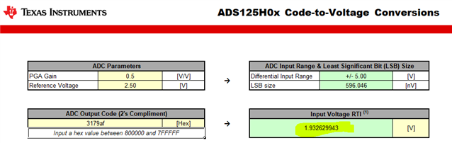
AIN0 - AINCOM and GAIN is 0.5 - which is 0v to +- 5v

my analog input to AIN0 is 1v and -0.5.

as far as now I'm getting the SPI response perfectly, but my issue is in RDATA

where I'm reading my output for this I have some questions 

In program - It is mandatory to give OFCAL and FULCAL register before RDATA and after START command.

In calculation - once I get my 24bit conversion for example:

AIN0 - 0.3 V

MSB - 31

MID - 79

LSB - AF

Then I converted this hex value into decimal and applied in formula - CONVERSION DATA * VREF / (2^24). 

Is this formula correct or not if it isn't then which formula to use.

does my procedure correct?

Or else will you please send me step by step procedure to single ended operation.

Previously I raised some questions but nothing changed.

So please help me out with this.

int main(void)
 {
    volatile uint32_t i;

    WDT_A->CTL = WDT_A_CTL_PW |             // Stop watchdog timer
            WDT_A_CTL_HOLD;

    P2->DIR |= BIT0;                        // Set P2.0 CS1
    P1->DIR |= BIT0;                        //CS2

    P2->SEL0 = BIT1 | BIT2 | BIT3;         // Set P2.1, P2.2, and P2.3 as
                                            // SPI pins functionality
    EUSCI_A1->CTLW0 |= EUSCI_A_CTLW0_SWRST; // Put eUSCI state machine in reset
    EUSCI_A1->CTLW0 = EUSCI_A_CTLW0_SWRST | // Remain eUSCI state machine in reset
            EUSCI_A_CTLW0_MST |             // Set as SPI master
            EUSCI_A_CTLW0_SYNC |            // Set as synchronous mode
            EUSCI_A_CTLW0_MSB;     // Set clock polarity high
    EUSCI_A1->CTLW0 &= ~EUSCI_A_CTLW0_CKPL;
    EUSCI_A1->CTLW0 &= ~EUSCI_A_CTLW0_CKPH;

    EUSCI_A1->CTLW0 |= EUSCI_A_CTLW0_SSEL__SMCLK; // ACLK
    EUSCI_A1->BRW = 0x0001;                   // /2,fBitClock = fBRCLK/(UCBRx+1).

    EUSCI_A1->CTLW0 &= ~EUSCI_A_CTLW0_SWRST;// Initialize USCI state machine

    // Enable global interrupt
    __enable_irq();

    /***** DEV_ID***/

   P2->OUT &= ~BIT0;
      
    write(0x20);

    write(0x00);

    write(0x79);

    write(0x00);

    write(0x00);

    write(0x00);
      
    P2->OUT |= BIT0;


    /****MODE-0***/
    P2->OUT &= ~BIT0;   // CS low
   
        write(0x42);

        write(0x24);

        write(0x5A);

        write(0x00);
 
    P2->OUT |= BIT0;


////    /***** MODE-1 ***/
    P2->OUT &= ~BIT0;   // CS low
    
        write(0x43);

        write(0x01);

        write(0xB4);

        write(0x00);
     
    P2->OUT |= BIT0;

      /***** REF ****/
    P2->OUT &= ~BIT0;   // CS low
    
        write(0x46);

        write(0x10);

        write(0x82);

        write(0x00);

    P2->OUT |= BIT0;
////
//      /***** MODE - 4*********/
    P1->OUT &= ~BIT0;   // CS low
        write(0x50);

        write(0x33);

        write(0x42);

        write(0x00);

    P1->OUT |= BIT0;

    while(1)
      {
               /**** start ****/
      P2->OUT &= ~BIT0;
          write(0x08);

          write(0x00);

          write(0x7F);

          write(0x00);

      P2->OUT |= BIT0;

      /********* RDATA *******/
      P2->OUT &= ~BIT0;   // CS low
      
           write(0x12);

           write(0x00);

           write(0xAA);

           write(0x00);

           write(0x00);

           write(0x00);

           write(0x00);

           write(0x00);

           write(0x00);
        
         P2->OUT |= BIT0;

           /**** STOP******/
        P2->OUT &= ~BIT0;
           write(0x0A);

           write(0x00);

           write(0x55);

           write(0x00);

            P2->OUT |= BIT0;

    }
}

  • Hi Sai,

    In our previous discussion, I had asked for the following:

    "Can you please read back the full register settings, then take data, and then post the register values as well as the data output? I cannot help much when I don't know how the ADC is configured and I cannot see the data output."

    At this point, this seems like a communication issue, so we need to be able to see what is being sent to the ADC and how the ADC responds in order to help. If G = 0.5 and VREF = 2.5V, then the value you are seeing (0x3179AFh) corresponds to 1.93V.

    You will need to provide oscilloscope or logic analyzer images of your communication as well.

    Please complete these tasks and provide us the requested information so we can continue assisting you.

    -Bryan

  • okay i will post and one more thing is, how you calculated (0x3179AFh) to 1.93V?

    what formula you used here? 

  • Hi Sai,

    I used the ADS125H02 Excel calculator tool and the gain / VREF information you have provided: https://www.ti.com/lit/zip/sbac234

    -Bryan

  • Isn't that the calculation only for differential output?

    because in ADC input range table in right side says differential input range.

    what i should use for single ended or same formula for both? 

  • hi,

    Today i did every possible ways to clear this issue but nothing changed.

    And I also tried the CRO to capture the signal but when every time I'm giving the values it is changing.

    for example : my AIN0 - 0.5 V

    MOSI - 12  00  AA  00  00  00  00  00  00

    MISO - FF  12  00  AA  00  B1  C2  24  FF

    EXAMPLE 2 :

    MOSI - 12  00  AA  00  00  00  00  00  00

    MISO - FF  12  00  AA  00  08  AA  15  FF

    my issue is especially MSB, MID, LSB only.

    My code is correct or not? Above I posted  my program.

    thanks in advance.

  • Hi Sai,

    As I mentioned in a previous thread, the ADC always takes a differential measurement. So if AIN0 is connected to 1V and AIN0 is connected to GND, the ADC reads 1V. If AIN0 is connected to 4V and AIN3 is connected to 3V, the ADC reads 1V.

    Similarly, the output coding is always bipolar, two's complement. So, for example, your first output code (0xB1C224h) corresponds to -3.056V if Gain = 0.5 and VREF = 2.5V. In your second example, 0x08AAFFh corresponds to 0.338V using the same settings.

    You still have not provided register read back information so we can see how the device is actually configured. Can you also send some pictures of your PCB setup and how everything is connected?

    -Bryan