This thread has been locked.

If you have a related question, please click the "Ask a related question" button in the top right corner. The newly created question will be automatically linked to this question.

ADC and FIFO integration

Other Parts Discussed in Thread: ADS62P49

Dear all,

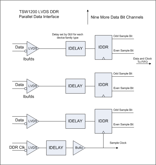
I am using 4DSP kit and in that I have TI ADC model ADS62p49.

Now The thing is that I am using channel 'a' of ADC which uses LVDS differentail clock and I want to inqure that since I want to capture that data to the FIFO should I use the differential to single ended buffer like the following code

Note that there is a IP defined to capture the data words, all I have to do is to utilize it at my will, first step of which is storing to FIFO.

-- IBUFDS: Differential Input Buffer
-- Virtex-6
-- Xilinx HDL Libraries Guide, version 13.2

IBUFDS_inst : IBUFDS generic map ( DIFF_TERM => FALSE, -- Differential Termination IBUF_LOW_PWR => TRUE, -- Low power (TRUE) vs. performance (FALSE) setting for refernced I/O standards IOSTANDARD => "DEFAULT") port map ( O => O, -- Buffer output I => I, -- Diff_p buffer input (connect directly to top-level port) IB => IB -- Diff_n buffer input (connect directly to top-level port) );


What I think this way I will be utilizing same clock both for Analog-to-Digital conversion and Data capturing to the FIFO.

What does the experience community fellows suggest. If there is any other better option please suggest.


Note: The FPGA is Virtex 6 and using ISE 13.2


Bests

Jaffry

  • Hi,

    Yes, you would instantiate the IBUFDS cell for the LVDS inputs.  in our TSW1200 we use this input cell and we do turn on the optional 100 ohm termination resistor to terminate the LVDS lines in the FPGA.  But after the IBUFDS, you still need something to latch the DDR (Dual Data Rate) data using both the rising and the falling edges of the clock.  Xilinx provides a cell called the IDDR that latches data on the falling and rising edges of the clock.  And then you have to make sure that you meet setup and hold timing into the IDDR cell, and Xilinx provides a cell called IDELAY that lets you delay either the data or the clock (or both) until setup and hold timing is met into the IDDR cell.  The static timing analysis tools in ISE13.2 and your timing constraints in your .ucf constraint file will help you determine if timing is met into the IDDR cells.

    After the data is properly latched by the IDDR cells, then you can latch the data into a FIFO or whatever other logic you care to define in your FPGA.

    Attached is a sketch of how we get the data from the ADC into the Virtex4 of the TSW1200.  For a 14bit DDR format such as ADS62P49 there would be 7 LVDS data pairs and the output of each of the 7 IDDR cells will be an odd-numbered data bit and an even numbered data bit from the sample.

    i don't know what you mean by your statement "this way I will be utilizing same clock both for Analog-to-Digital conversion and Data capturing to the FIFO" .  The sample clock to the ADC must be a very clean, low-jitter low-phase noise differential clock signal.  Having the FPGA source the clock to the ADC will likely hurt the SNR performance of the ADC.  Given an external clean sample clock to the ADC, the ADC will then output an LVDS clock with the LVDS sample data, and the LVDS output clock will be the same frequency as the sample clock. So the digital path from the ADC into the FPGA is LVDS clock with data, and you will need to implement an LVDS DDR  interface similar to the attached sketch using this clock and data. 

    Regards,

    Richard P.

  • Thank you for your response.

    Well O.K. once I am able to get the data. What I mean by "this way I will be utilizing same clock both for Analog-to-Digital conversion and Data capturing to the FIFO" is that I want to give exactly same clock to the FIFO as to the ADC or IDDR. (of course single ended)

    What do you suggest.

  • If you supply a clock to the ADC and then supply that same clock to the FPGA to latch the sample data, you have to be careful of the min to max propagation delay through the ADC.  The min to max prop delay through the ADC will subtract from your timing margin going into the FPGA.  From the datasheet:

    Given that there is 3 ns of min to max propagation variance through the ADC to subtract from your setup adn hold margin into the ADC, I don't think this will work.  I think you will need to supply a clock to the ADC, and then use the LVDS output clock with the sample data into the FPGA.  This LVDS output clock with the sample data is at the same rate as the sample clock, but its timing will be matched with the data bus.

    Regards,

    Richard P.

  • Shan,

    The 4DSP folks also indicated that you can use the 4DSP kit serial number to subscribe for extra support from the 4DSP forum:

    http://www.4dsp.com/forum/

    This may be a good resource as well since they can support that exact kit/interface and may already have sample code/projects to help you out further.

    Ken