This thread has been locked.

If you have a related question, please click the "Ask a related question" button in the top right corner. The newly created question will be automatically linked to this question.

ADS1255

Other Parts Discussed in Thread: ADS1251, ADS1255, ADS1252

Hello,

first of all please be patient, my english wasn't used for a long time.

I'm a little bit in trouble. I'm writing my bachelor thesis an one part of it is a pressure sensor whose data i will convert via the 1255 and then send the data to an Arduino Nano board (ATMega 328).

The problem is i always have zeros in my SPDR register (the place where the bytes should be transfered).

First i evaluated the adc with the evalboard and there it worked well but now i have an ADC1255 on a board, with the pressure sensor next to him and it doesn't!

So i belive i haven't set up the right configuration (of have set up the right configuration in a wrong way!?)

When i now try to configure the adc and collect data, i always get zeros. I really don'k know if i'm doing it right, so i hope you can help me with this.

My SPI configuration on the µC is:

  • MSB first,
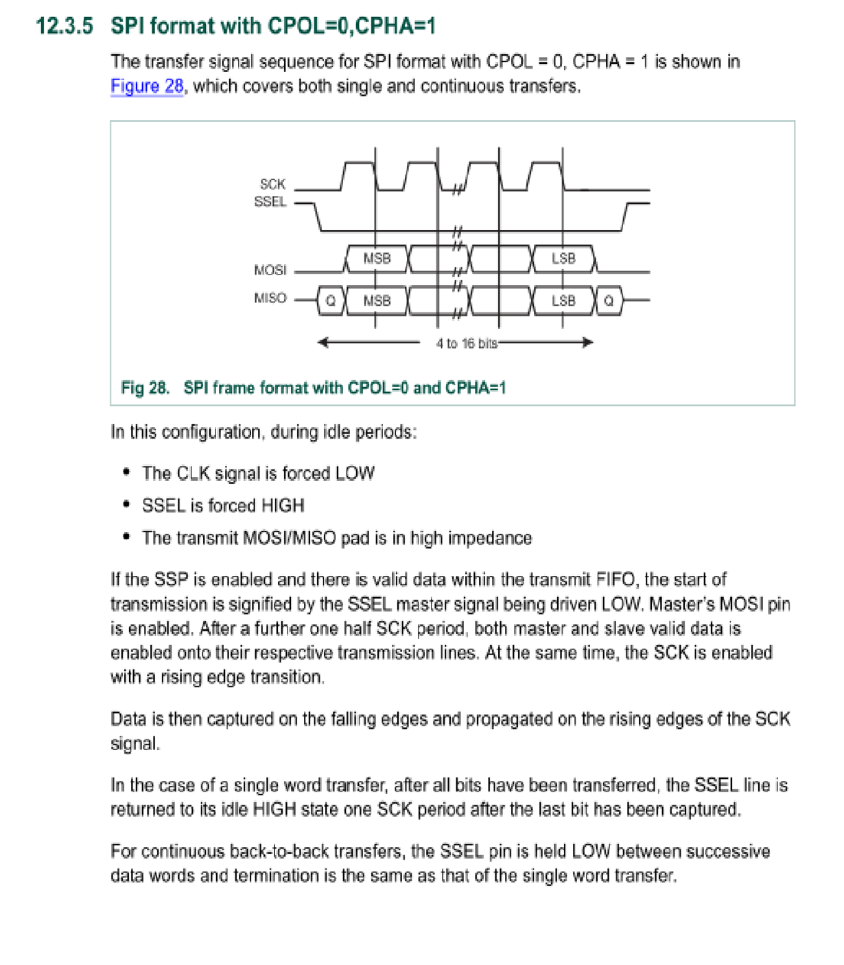
  • SPI_Mode1 (low when idle, falling edge)
  • clockspeed is 8MHz

here is the code for the configuration (the SPI.transfer function is from the arduino library):

  SPI.transfer(0x00);        //wakeup 
  SPI.transfer(0x0F);        //stop reading continously if so 
  SPI.transfer(0xFE);       //reset
  SPI.transfer(0x510001);      //Write(5) register(1),Number of Data(0) Number(0), Databyte (01)   --> AIN0 & AIN 1
  SPI.transfer(0x520004);       //Write(5) register(2),Number of Data(0) Number(0), Databyte (04)  --> PGA = 16
  SPI.transfer(0x530003);       //Write(5) register(1),Number of Data(0) Number(0), Databyte (03)  --> 2.5 sps 
  SPI.transfer(0xFC);        //synchronize 
  SPI.transfer(0xF1);        //Offset self calibration 
  SPI.transfer(0xF2);        //Gain self calibration 
  SPI.transfer(0xF3);        //System offset self calibration 
  SPI.transfer(0xF4);        //System gain self calibration                                                                                  
  SPI.transfer(0xFC);        //synchronize 
  SPI.transfer(0xFF);        //wakeup

in the loop i try to read out the bytes

SPI.transfer(0x01);
// wait until data is shifted out
delayMicroseconds(1);       //50x t_clk 
  //read from SPI Register
  buffer[0] = SPDR;
  buffer[1] = SPDR;
  buffer[2] = SPDR;

Here is another question. How can i manage to read out 3 byte out of an one byte register? I hoped that it will be shifted in, after i read the byte, but how can i know?!

When i read the DOUT with the Osci i always get a flatline. Even if i send a commant to read a register i stays zero.

Can you pleasy help me with that problem? I'm running out of time.

Thanks
Dennis Zimmermann

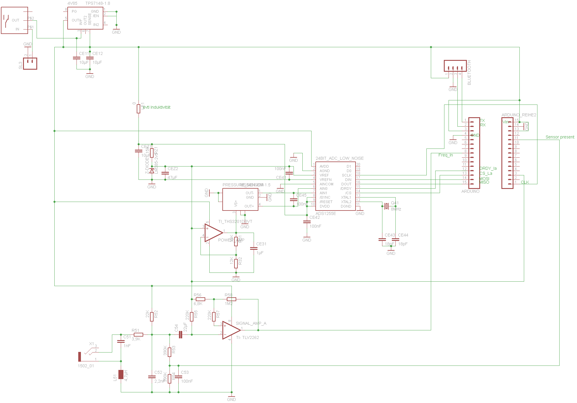
PS: i attached my scematic. I don't belive it's a layout problem but maybe for you it's better to understand what i am doing

  • Hi Dennis,

    First think I would do is verify that you are getting /DRDY pulses out of the part. This will tell you that the device is up and running correctly updating the output register as each conversion completes. You should see pulses similar in width to what is shown in Figure 4 of the data sheet.

    The output data word is going to consist of three bytes with eight bits per byte. Depending on whether you decide to use read data continuous mode or read data per the command will determine how you can read data out. It looks like in your code steps you listed above, you are taking the device out of read data continuous mode (RDATAC) in your second SPI transfer item and then attempting to use the RDATA command whenever you are ready to read back data. That is a fine approach to take, just make sure that you are using the /DRDY as an interrupt to know when to send the RDATA command to begin reading back data. Once the RDATA command is sent, you need to send 24 SCLKs in order to read the data back.

    It is hard for me to see your schematic. Do you mind attaching it as a file using the 'options' --> 'File attach' in the forum post.

    Regards,

    Tony Calabria

  • Hi Dennis!

    Welcome to the e2e forum!  We'll take a look over your code and schematic for the ADS1255.  In the meantime, here is an app note on setting up the ADS1251 and ADS1252 with one of our MSP430 devices that might help you out.  The ADS1251 and ADS1252 are single channel parts with a similar command structure and SPI interface to the ADS1255.

    http://focus.ti.com/lit/an/slaa242/slaa242.pdf

  • Hi Tony,

    Thanks for the response!

    I am getting the /DRDY pulses. In my code i'm waiting for the falling edge

     do
      {}
      while (digitalRead(dataReadyPin) == HIGH);

    I've made a few more meassures and it seems as the DOUT line is always zero. Even when i send the RREG command to read out the status register, DOUT stays low.

    SPI.transfer(0x1000);
    SPI.transfer(0xAA);

    (for being shure there is a clock to shift data out i send 0xAA)

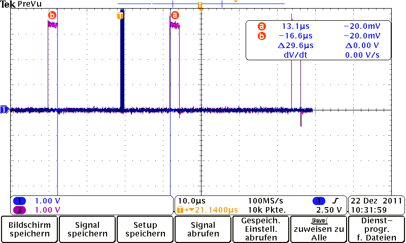
    In the attachment i've put two images of the scope, where the /DRDY is clear to see, and another with the RDATA command.

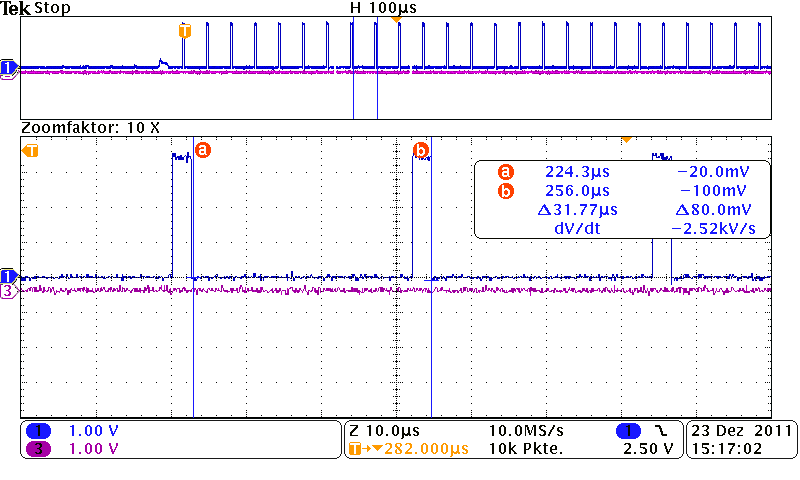
    Remarkable on the /DRDY image is that the period of the peaks is 30µs ~> 30000 sps (running with 8MHz). in the setup i tried to settle the ads down to 2,5sps. It seems like all my commands doesn't work and the ads is running in it's default mode.

    Have you any idea?

    Thanks

    Dennis Zimmermann

  • additional note:

    all the signals were meassured at the pins of the adc.

    regards

    Dennis Zimmermann

  • Hi Dennis,

    Establishing communication between the ADC and your uC is the first step. If the data rate (time between DRDY falling edges) is not changing when you are changing the data rate bits in the registers, you probably have a bug in the communication. First thing to check is to make sure that you have your clock phasing and polarity correct in that you are configured to use the falling edge of SCLK as the critical edge to latch data into DIN and using the rising edge of SCLK for data to change. Make sure you are bringing /CS low during all your transmissions.First transmission test I would run is put the device in standby mode and then wake it up using commands.While in Standby mode, the DRDY should just idle high and not pulse. This would tell you if you are getting commands into the converter correctly.

    Standby command -0xFD

    Wait for seconds or longer to verify that DRDY is idling high

    Wakeup command - 0xFF

    Once communication is working, use the list below to put the device in SDATAC mode, then write to change the data rate -

    0x0F - Put part is SDATAC mode

    0x530003 - Write to change the data rate. (do not send a reset command before)

    After you write this command and when you start the conversions, you should see duration between DRDY pulses change to the desired data rate.


    Regards,

    Tony Calabria

  • Hello!

    I tried to set the adc into standby and it is working.

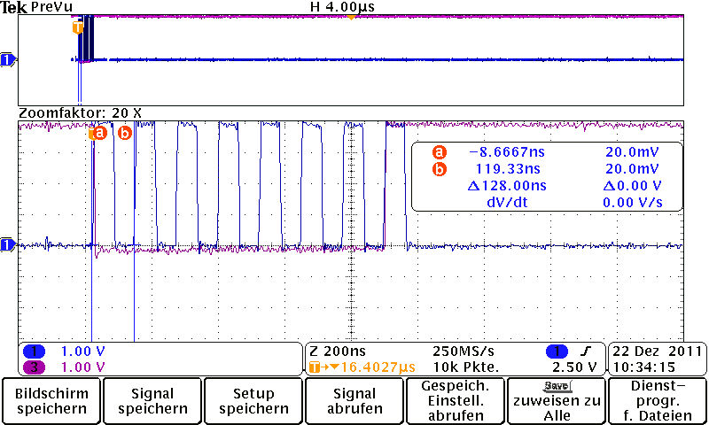
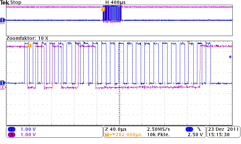
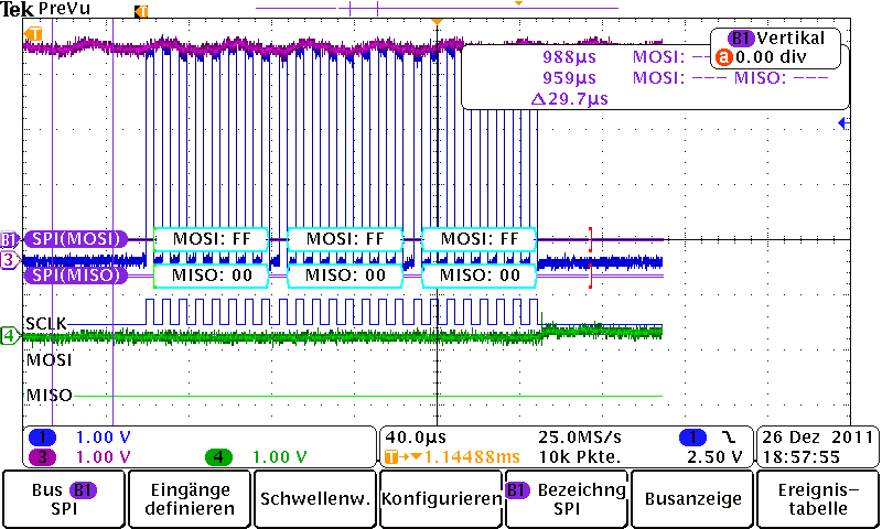
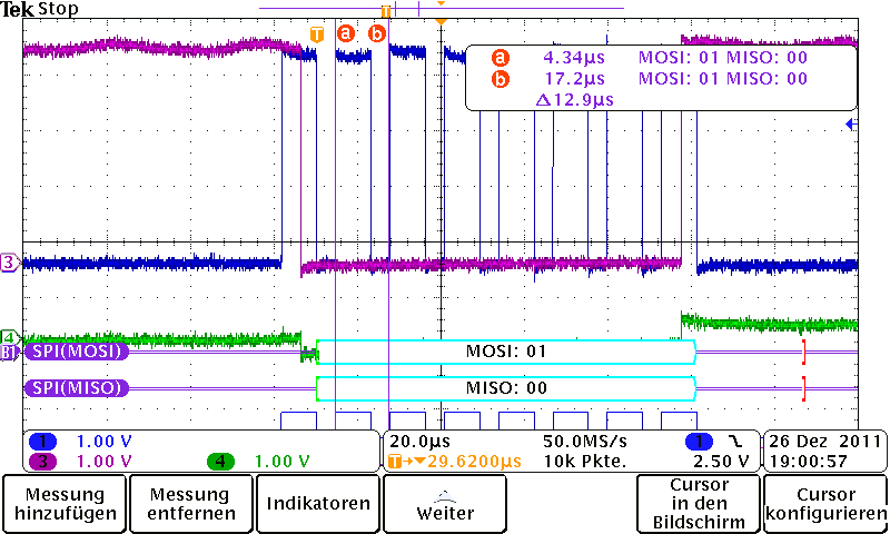
    I think that there is a problem in transmitting 3 bytes in a row. In the datasheet it is remarked that the second (and  third) byte must be shifted out without delay. When i use the SPI library there is a little pause between the two bytes, so i wrote my own SPI function. This function sends 24 bit without any delay between the bytes. The clock period is ~ 17µs and the bits are stable on the falling edge (see attachment).

    As you can see on the image, i'm sending 0x530003 -> 2.5sps

    the next attachment shows my /DRDY signal (same configuration). It is still a 30ksps period. My commands seem to be meaningless. The only one that works is a one byte command.

    How can i manage this problem?

    Regards

    Dennis Zimmermann

  • Hello again.

    Now i solved the problem with the comands. I implemented my own SPI class. Now i can manage to switch the sps and others.

    But i still have the problem, that the output is always zero. I've set the PGA up to 64 and even if i put 3V to one of the AIN's (regular ~2V on both) , there is noch change.

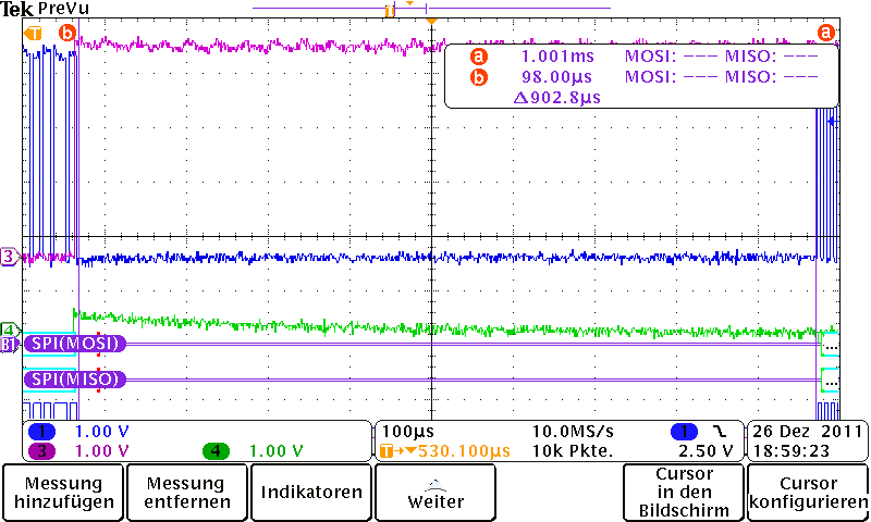
    The time between the readData (0x01) and the measure at the DOUT is 1ms at a clocktime of about 10-20µs. Time between /DRDY is 380ms (2.5sps @ 8MHz).

    I attached some Osci images for better understanding.

    Picture one shows the DIN & DOUT after sending RDATA

    Picture two shows the timing t6 from sending the request to collecting the data (>50 t_clk)

    Picture three shows the clockperiod.

    Please help me with this ***... i'm running into serious trouble if i can't solve the problem.

    Thanks a lot

    Dennis

  • Hi Dennis,

    Can you repeat the pictures above while including the /CS input?  You can turn off the zoom functions and menus.  Have you also verifired your reference voltage?

  • Hi!

    /CS is always low.

    My reference Voltage is 2.0V (via Z-Diode)

    Changing the settings is working now. But i dont get any value out of this black box.

  • Hello again!

    You were right... at least it seems so. I connected GND to the VREFP, and my 2V to VREFN. I haven't tested it yet, but i think that is the (mayor) problem.

    Thanks for your help!

    Regards

    Dennis

  • Hi again Dennis!

    Having the reference reversed could certainly cause the problems you've seen with the conversion results.  Let us know what you see when after you had a chance to test it out with the revised wiring.

  • Hi There

    I am facing the same problem as Dennis mentioned. I tested the SPI communication using STANDY command and it works . Therefore when I try to read something frmo the registers it returns always 0 (flatline).

    Here is the piece of code to read the registers
    /*******************************************************************************
    * Function : ADS1255_ReadReg *
    * In Parameter : unsigned byte , unsigend byte *
    * Out Parameter : unsigned byte *
    * Description : Perform Desired Register Reading *
    *******************************************************************************/
    u8 Ads1255ReadReg ( u8 reg, u8 conv )
    {
    u8 regTemp;
    switch ( conv ) //turn on the right A/D Converter
    {
    case AD_SAGNAG:
    IO0CLR |= CS_SAG;
    IO0SET |= CS_SOMA;
    break;
    case AD_SOMA:
    IO0CLR |= CS_SOMA;
    IO0SET |= CS_SAG;
    break;
    }
    ssp_send_byte ( 0x10 | reg );
    Delay1us(3);
    ssp_send_byte ( 0x00 ); //only one register
    regTemp = ssp_read_byte();
    //regTemp = -(regTemp >> 3);
    Delay1us(5);

    switch ( conv ) //turn off the right A/D Converter
    {
    case AD_SAGNAG:
    IO0SET |= CS_SAG;
    break;
    case AD_SOMA:
    IO0SET |= CS_SOMA;
    break;
    }
    return ( regTemp );
    }

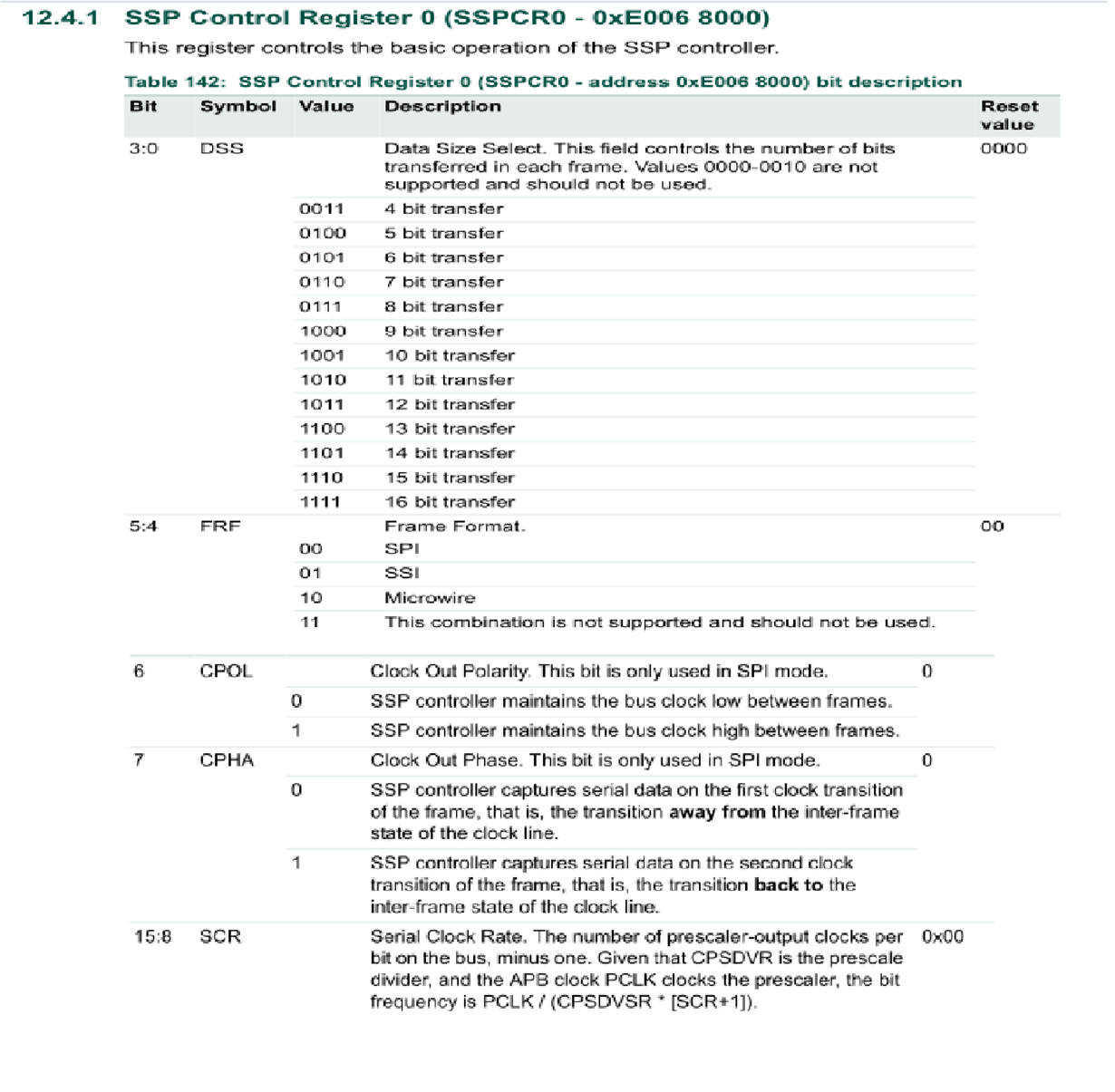
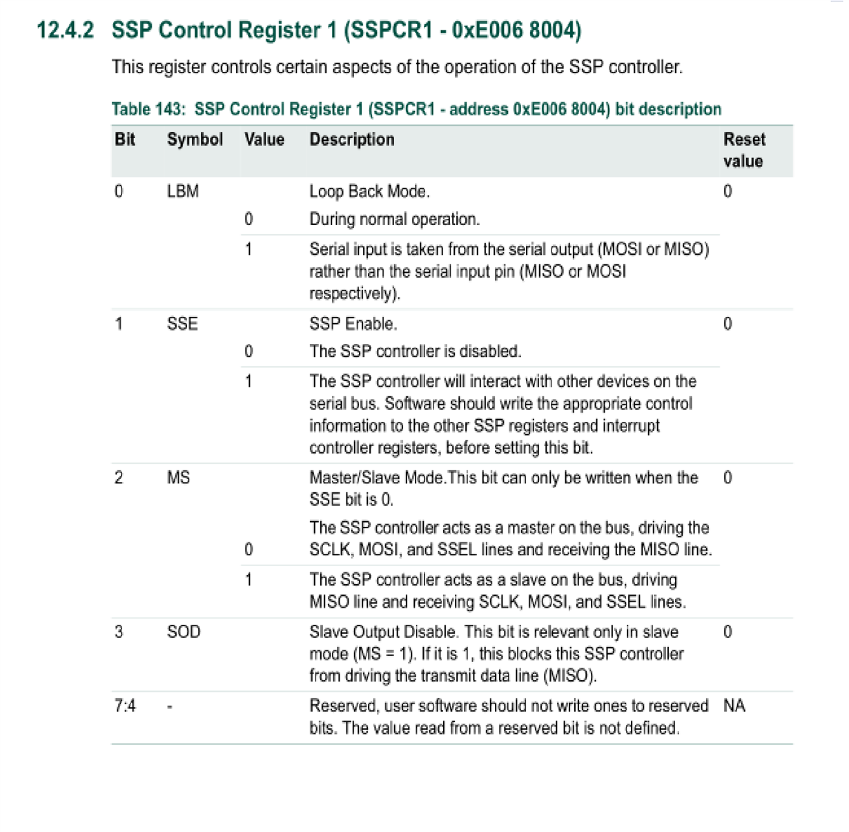
    I am using LPC2132 Processor and my SPI settings are : SPI Mode 1, SCLK 0.96MHz. The CLKIN is equal 7.68Mhz.

    Any help , clue or tips are really welcome , sicen I am running in short time
  • Hi Shigueru,

    Have you looked at the SPI pins on a scope or logic analyzer to verify that your code is doing what you expect it to?

    Make sure you are not in RDATAC mode when reading or writing to the device registers (you many need to send the SDATAC command first, to make sure that you exit this mode).

    Other than that I would suggest adding a short delay (>50ns) after setting /CS low, and perhaps increasing your 3us delay to 6us to satisfy the t6 timing requirement.

    Best Regards,
    Chris
  • Hi Chris

    Thanks for the fast reply

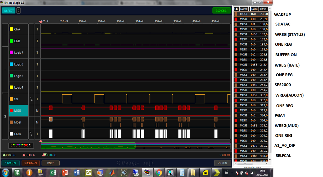
    Here is the logic analyzer screensahoot ( in the rightr side i insert the sequence that I am using to initialize the ADS 1255). Do you see anything worng ?

    Inserted the ADS1255.h and ADS1255.c files too.

    H FILE ////////////////////////////////////////////////////////////////////////////////////////////////////////////////////////////////////////////////////////////////////////////////////////////////////////////////////////////////////////////////////////////////////////////

    #define _ADS1255_H_
    /*******************************************************************************
    * INCLUDES *
    *******************************************************************************/
    #include <LPC213X.H>
    #include "types.h"
    #include "ssp.h"
    #include "hardware.h"
    #include "util.h"
    /*******************************************************************************
    * DEFINES *
    *******************************************************************************/
    #define R_STATUS 0x00

    #define BUFFER_ON 0x02
    #define BUFFER_OFF 0x00

    #define R_MUX 0x01
    #define A0_A1_DIF 0x01
    #define A1_A0_DIF 0x10
    #define A0_COMUM 0x08
    #define A1_COMUM 0x18

    #define R_ADCON 0x02
    #define PGA1 0
    #define PGA2 1
    #define PGA4 2
    #define PGA8 3
    #define PGA16 4

    #define R_DRATE 0x03
    #define SPS30000 0xF0
    #define SPS15000 0xE0
    #define SPS7500 0xD0
    #define SPS3750 0xC0
    #define SPS2000 0xB0 //15 internal averages
    #define SPS1000 0xA1 //30 internal averages
    #define SPS500 0x92
    #define SPS100 0x82 //300 averages
    #define SPS10 0x23 //3000 averages
    #define SPS5 0x13 //6000 internal averages
    #define SPS2_5 0x03

    #define R_IO 0x04
    #define R_OFC0 0x05
    #define R_OFC1 0x06
    #define R_OFC2 0x07
    #define R_FSC0 0x08
    #define R_FSC1 0x09
    #define R_FSC2 0x0A

    #define C_WAKEUP 0x00 //Leave standby
    #define C_RDATA 0x01 //Read Unique Converted Data
    #define C_RDATAC 0x03 //Read Conversion Conversion Continuously
    #define C_SDATAC 0x0F //Stop continuos reading
    #define C_SELFCAL 0xF0 //Offset and Gain Self-Calibration
    #define C_SELFOCAL 0xF1 //Offset Self-Calibration
    #define C_SELFGCAL 0xF2 //Gain Self-Calibration
    #define C_SYSOCAL 0xF3 //System Offset Calibration
    #define C_SYSGCAL 0xF4 //System Gain Calibration
    #define C_SYNC 0xFC //System Gain Calibration
    #define C_STDBY 0xFD //StandBy Mode
    #define C_RESET 0xFE //Reset up Power Values

    #define AD_SAGNAG 0
    #define AD_SOMA 1

    #define PGAmulti_1 0.0000005960464832810452 //PGA-1 ±5V
    #define PGAmulti_2 0.0000002980232416405226 //PGA-2 ±2.5V
    #define PGAmulti_4 0.0000001490116208202613 //PGA-4 ±1.25V
    #define PGAmulti_8 0.00000007450581041013064 //PGA-8 ±0.625V
    #define PGAmulti_16 0.00000003725290520506532 //PGA-16 ±312.5mV
    #define PGAmulti_32 0.00000001862645260253266 //PGA-32 ±156.25mV
    #define PGAmulti_64 0.000000009313226301266331 //PGA-64 ±78.125mV

    /*******************************************************************************/
    /* PROTOTYPES */
    /*******************************************************************************/
    void Ads1255Init ( void );
    void Ads1255SelfCal (u8 conv);
    void Ads1255WriteReg (u8 reg, u8 data, u8 conv);
    void Ads1255ReadAd(u8 conv,i32_8 temp);
    void Ads1255SelfOcal(u8 conv);
    void Ads1255SysOcal(u8 conv);
    void Ads1255_MUX (u8 conv);
    u8 Ads1255ReadReg ( u8 reg, u8 conv );
    void Ads1255WakeUp( u8 conv );
    void Ads1255Sync( u8 conv );
    void Ads1255_Stdby( u8 conv );
    void Ads1255_SdataC( u8 conv );

    #endif

    C FILE////////////////////////////////////////////////////////////////////////////////////////////////////////////////////////////////////////////////////////////////////////////////////////////////////////////////////////////////////////////////////////////////////////////

    /*******************************************************************************
    * INCLUDES *
    *******************************************************************************/
    #include "ads1255.h"


    /*******************************************************************************
    * PROTOTYPES *
    ********************************************************************************/

    /*******************************************************************************
    * Function : ADS1255_Init *
    * In Parameter : None *
    * Out Parameter : None *
    * Description : Activating and Configuration for both ADS1255 Circuits *
    ********************************************************************************/
    void Ads1255Init ( void)
    {
    // u8 status_reg;
    IO0CLR |= AD_RESET ;
    Delay1us(200);
    IO0SET |= AD_RESET;
    DelayMs(2);

    // Ads1255_Stdby(AD_SAGNAG);
    // DelayMs(300);
    Ads1255WakeUp(AD_SAGNAG);
    Delay1us(10);
    Ads1255_SdataC(AD_SAGNAG);
    Delay1us(10);
    //Config SagNag A/D Converter
    Ads1255WriteReg ( R_STATUS, BUFFER_ON, AD_SAGNAG );
    Ads1255WriteReg ( R_DRATE, SPS2000, AD_SAGNAG ); //2000sps
    Ads1255WriteReg ( R_ADCON, PGA4 , AD_SAGNAG ); //PGA=4,clkout=off
    Ads1255WriteReg ( R_MUX, A1_A0_DIF, AD_SAGNAG );
    Delay1us(10);
    Ads1255SelfCal (AD_SAGNAG);
    Delay1us(10);

    Ads1255WakeUp(AD_SOMA);
    Delay1us(10);
    Ads1255_SdataC(AD_SOMA);
    Delay1us(10);

    //Config Soma
    Ads1255WriteReg ( R_STATUS, BUFFER_OFF , AD_SOMA );
    Ads1255WriteReg ( R_DRATE, SPS2000, AD_SOMA ); //100sps
    Ads1255WriteReg ( R_ADCON, PGA1 , AD_SOMA );
    Ads1255WriteReg ( R_MUX, A1_COMUM, AD_SOMA);
    Delay1us(10);
    Ads1255SelfCal (AD_SOMA);
    Delay1us(10);

    IO0CLR |= AD_SYNC;
    Delay1us(50);
    IO0SET |= AD_SYNC;
    Delay1us(100);
    //status_reg = Ads1255ReadReg(R_STATUS, AD_SAGNAG);
    Delay1us(10);
    IO0SET |= (CS_SAG | CS_SOMA);

    }

    /*******************************************************************************
    * Function : ADS1255_WriteReg *
    * In Parameter : unsigned char,unsigned byte,unsigned char *
    * Out Parameter : None *
    * Description : Writing into A/D Registers *
    ********************************************************************************/
    void Ads1255WriteReg ( u8 reg, u8 data, u8 conv )
    {
    u8 reg_data;
    reg_data = 0x50|reg;
    switch ( conv ) // Turn on the right CS
    {
    case AD_SAGNAG:
    IO0CLR |= CS_SAG;
    IO0SET |= CS_SOMA;
    break;
    case AD_SOMA:
    IO0CLR |= CS_SOMA;
    IO0SET |= CS_SAG;
    break;
    }
    Delay1us(5);
    ssp_send_byte (reg_data);
    ssp_send_byte (0x00);
    ssp_send_byte (data);
    Delay1us(5);

    IO0SET |= CS_SAG;
    IO0SET |= CS_SOMA;


    }
    /*******************************************************************************
    * Function : ADS1255_SelfCal *
    * In Parameter : unsigned byte *
    * Out Parameter : None *
    * Description : Perform Self Calibration in A/D Circuit *
    ********************************************************************************/
    void Ads1255SelfCal ( u8 conv )
    {
    switch ( conv ) // Turns on the right CS
    {
    case AD_SAGNAG:
    IO0CLR |= CS_SAG;
    break;
    case AD_SOMA:
    IO0CLR |= CS_SOMA;
    break;
    }
    Delay1us(10);
    ssp_send_byte ( C_SELFCAL );
    Delay1us(10);

    if ( conv == AD_SAGNAG )
    while ( (IO0PIN && 0x100000)== 0x100000); //==1
    else
    while ( (IO0PIN && 0x40000000)==0x40000000); //==1

    IO0SET |= CS_SOMA|CS_SAG; //desligar CS dos ADs
    }

    /*******************************************************************************
    * Function : ADS1255_ReadAd *
    * In Parameter : unsigned byte *
    * Out Parameter : i32 *
    * Description : Read value from a selected A/D Converter *
    *******************************************************************************/
    void Ads1255ReadAd ( u8 conv , i32_8 temp)
    {
    switch ( conv )
    {
    case AD_SAGNAG:
    IO0CLR |= CS_SAG;
    while(AD_DRDY_SAG);
    break;
    case AD_SOMA:
    IO0CLR |= CS_SOMA;
    while(AD_DRDY_SOMA);
    break;
    }
    if ( conv == AD_SAGNAG )
    while ( (IO0PIN && 0x100000)== 0x100000); //==1
    else
    while ( (IO0PIN && 0x40000000)==0x40000000); //==1
    ssp_send_byte (C_RDATA);
    Delay1us(1);
    temp.i8[3] = 0;
    temp.i8[2] = ssp_read_byte();
    temp.i8[1] = ssp_read_byte();
    temp.i8[0] = ssp_read_byte();

    if ((0x80 & temp.i8[2]) == 0x80)
    temp.i8[3] = 0xFF;

    IO0SET |= CS_SOMA|CS_SAG;
    }

    /*******************************************************************************
    * Function : ADS1255_SelfOCal *
    * In Parameter : unsigned byte *
    * Out Parameter : None *
    * Description : Perform Self Offset in A/D Circuit *
    *******************************************************************************/
    void Ads1255SelfOcal (u8 conv)
    {
    switch ( conv )
    {
    case AD_SAGNAG:
    IO0CLR = CS_SAG;
    break;
    case AD_SOMA:
    IO0CLR = CS_SOMA;
    break;
    }
    Delay1us(10);
    ssp_send_byte( C_SELFOCAL );

    if (conv == AD_SAGNAG )
    while ( (IO0PIN && 0x100000)== 0x100000); //==1
    else
    while ( (IO0PIN && 0x40000000)==0x40000000); //==1
    Delay1us(10);
    IO0SET |= CS_SOMA|CS_SAG;
    }
    /*******************************************************************************
    * Function : ADS1255_SysOCal *
    * In Parameter : unsigned byte *
    * Out Parameter : None *
    * Description : Perform System Offset in A/D Circuit *
    *******************************************************************************/
    void Ads1255SysOcal(u8 conv)
    {
    switch ( conv )
    {
    case AD_SAGNAG:
    IO0CLR = CS_SAG;
    break;
    case AD_SOMA:
    IO0CLR = CS_SOMA;
    break;
    }
    Delay1us(10);
    ssp_send_byte ( C_SYSOCAL );
    if ( conv == AD_SAGNAG )
    while ( (IO0PIN && 0x100000)== 0x100000); //==1
    else
    while ( (IO0PIN && 0x40000000)==0x40000000); //==1
    Delay1us(10);
    IO0SET |= CS_SOMA|CS_SAG;
    }
    /*******************************************************************************
    * Function : ADS1255_MUX *
    * In Parameter : unsigned byte *
    * Out Parameter : None *
    * Description : Perform Multiplexer Operation *
    *******************************************************************************/
    void Ads1255_MUX (u8 conv)
    {
    switch ( conv )
    {
    case AD_SAGNAG:
    IO0CLR = CS_SAG;
    break;
    case AD_SOMA:
    IO0CLR = CS_SOMA;
    break;
    }
    Delay1us(10);
    ssp_send_byte (C_SYNC);
    Delay1us(10);
    ssp_send_byte (C_WAKEUP);
    Delay1us(10);
    ssp_send_byte (C_RDATA);
    Delay1us(10);

    IO0SET |= CS_SOMA|CS_SAG;
    }

    /*******************************************************************************
    * Function : ADS1255_ReadReg *
    * In Parameter : unsigned byte , unsigend byte *
    * Out Parameter : unsigned byte *
    * Description : Perform Desired Register Reading *
    *******************************************************************************/
    u8 Ads1255ReadReg ( u8 reg, u8 conv )
    {
    u8 regTemp;
    switch ( conv ) //turn on the right A/D Converter
    {
    case AD_SAGNAG:
    IO0CLR |= CS_SAG;
    IO0SET |= CS_SOMA;
    break;
    case AD_SOMA:
    IO0CLR |= CS_SOMA;
    IO0SET |= CS_SAG;
    break;
    }
    Delay1us(1);
    ssp_send_byte ( 0x10 | reg );
    Delay1us(6);
    ssp_send_byte ( 0x00 ); //only one register
    regTemp = ssp_read_byte();
    //regTemp = -(regTemp >> 3);
    Delay1us(5);

    switch ( conv ) //turn off the right A/D Converter
    {
    case AD_SAGNAG:
    IO0SET |= CS_SAG;
    break;
    case AD_SOMA:
    IO0SET |= CS_SOMA;
    break;
    }
    return ( regTemp );
    }

    /*******************************************************************************
    * Function : ADS1255_WakeUp *
    * In Parameter : unsigned byte *
    * Out Parameter : None *
    * Description : Perform WakeUp in A/D Circuit *
    ********************************************************************************/
    void Ads1255WakeUp( u8 conv )
    {
    switch ( conv ) // Turns on the right CS
    {
    case AD_SAGNAG:
    IO0CLR |= CS_SAG;
    IO0SET |= CS_SOMA;
    break;
    case AD_SOMA:
    IO0CLR |= CS_SOMA;
    IO0SET |= CS_SAG;
    break;
    }
    Delay1us(10);
    ssp_send_byte ( C_WAKEUP );
    Delay1us(10);

    switch ( conv ) // Turns off the right CS
    {
    case AD_SAGNAG:
    IO0SET |= CS_SAG;
    break;
    case AD_SOMA:
    IO0SET |= CS_SOMA;
    break;
    }
    }
    /*******************************************************************************
    * Function : ADS1255_Sync *
    * In Parameter : unsigned byte *
    * Out Parameter : None *
    * Description : Perform Sync in A/D Circuit *
    *******************************************************************************/
    void Ads1255Sync( u8 conv )
    {
    switch ( conv ) // Turns on the right CS
    {
    case AD_SAGNAG:
    IO0CLR |= CS_SAG;
    IO0SET |= CS_SOMA;
    break;
    case AD_SOMA:
    IO0CLR |= CS_SOMA;
    IO0SET |= CS_SAG;
    break;
    }
    Delay1us(2);
    ssp_send_byte ( C_SYNC );
    Delay1us(2);

    switch ( conv ) // Turns off the right CS
    {
    case AD_SAGNAG:
    IO0SET |= CS_SAG;
    break;
    case AD_SOMA:
    IO0SET |= CS_SOMA;
    break;
    }
    }
    /*******************************************************************************
    * Function : ADS1255_Stdby *
    * In Parameter : unsigned byte *
    * Out Parameter : None *
    * Description : Put A/D Circuit in StandBy Mode *
    *******************************************************************************/
    void Ads1255_Stdby( u8 conv )
    {
    switch ( conv ) // Turns on the right CS
    {
    case AD_SAGNAG:
    IO0CLR |= CS_SAG;
    IO0SET |= CS_SOMA;
    break;
    case AD_SOMA:
    IO0CLR |= CS_SOMA;
    IO0SET |= CS_SAG;
    break;
    }
    Delay1us(10);
    ssp_send_byte ( C_STDBY );
    Delay1us(10);

    switch ( conv ) // Turns off the right CS
    {
    case AD_SAGNAG:
    IO0SET |= CS_SAG;
    break;
    case AD_SOMA:
    IO0SET |= CS_SOMA;
    break;
    }
    }
    /*******************************************************************************
    * Function : ADS1255_SdataC *
    * In Parameter : unsigned byte *
    * Out Parameter : None *
    * Description : Put A/D Circuit in StandBy Mode *
    *******************************************************************************/
    void Ads1255_SdataC( u8 conv )
    {
    if ( conv == AD_SAGNAG )
    while ( (IO0PIN && 0x100000)== 0x100000); //==1
    else
    while ( (IO0PIN && 0x40000000)==0x40000000); //==1

    switch ( conv ) // Turns on the right CS
    {
    case AD_SAGNAG:
    IO0CLR |= CS_SAG;
    IO0SET |= CS_SOMA;
    break;
    case AD_SOMA:
    IO0CLR |= CS_SOMA;
    IO0SET |= CS_SAG;
    break;
    }
    Delay1us(10);
    ssp_send_byte ( C_SDATAC );
    Delay1us(10);

    switch ( conv ) // Turns off the right CS
    {
    case AD_SAGNAG:
    IO0SET |= CS_SAG;
    break;
    case AD_SOMA:
    IO0SET |= CS_SOMA;
    break;
    }
    }

    Sorry to bother you. I am running in short time with this task and I was empty of ideas to solve this. 

    Thanks

    Shigueru

  • Thanks Chris.

    I will check it.
    Here is the source code that I am using

    ////////////////////////////////////////////////////HEADER FILE////////////////////////////////////////////////////////////////////////////////////
    #define _ADS1255_H_
    /*******************************************************************************
    * INCLUDES *
    *******************************************************************************/
    #include <LPC213X.H>
    #include "types.h"
    #include "ssp.h"
    #include "hardware.h"
    #include "util.h"
    /*******************************************************************************
    * DEFINES *
    *******************************************************************************/
    #define R_STATUS 0x00

    #define BUFFER_ON 0x02
    #define BUFFER_OFF 0x00

    #define R_MUX 0x01
    #define A0_A1_DIF 0x01
    #define A1_A0_DIF 0x10
    #define A0_COMUM 0x08
    #define A1_COMUM 0x18

    #define R_ADCON 0x02
    #define PGA1 0
    #define PGA2 1
    #define PGA4 2
    #define PGA8 3
    #define PGA16 4

    #define R_DRATE 0x03
    #define SPS30000 0xF0
    #define SPS15000 0xE0
    #define SPS7500 0xD0
    #define SPS3750 0xC0
    #define SPS2000 0xB0 //15 internal averages
    #define SPS1000 0xA1 //30 internal averages
    #define SPS500 0x92
    #define SPS100 0x82 //300 averages
    #define SPS10 0x23 //3000 averages
    #define SPS5 0x13 //6000 internal averages
    #define SPS2_5 0x03

    #define R_IO 0x04
    #define R_OFC0 0x05
    #define R_OFC1 0x06
    #define R_OFC2 0x07
    #define R_FSC0 0x08
    #define R_FSC1 0x09
    #define R_FSC2 0x0A

    #define C_WAKEUP 0x00 //Leave standby
    #define C_RDATA 0x01 //Read Unique Converted Data
    #define C_RDATAC 0x03 //Read Conversion Conversion Continuously
    #define C_SDATAC 0x0F //Stop continuos reading
    #define C_SELFCAL 0xF0 //Offset and Gain Self-Calibration
    #define C_SELFOCAL 0xF1 //Offset Self-Calibration
    #define C_SELFGCAL 0xF2 //Gain Self-Calibration
    #define C_SYSOCAL 0xF3 //System Offset Calibration
    #define C_SYSGCAL 0xF4 //System Gain Calibration
    #define C_SYNC 0xFC //System Gain Calibration
    #define C_STDBY 0xFD //StandBy Mode
    #define C_RESET 0xFE //Reset up Power Values

    #define AD_SAGNAG 0
    #define AD_SOMA 1

    #define PGAmulti_1 0.0000005960464832810452 //PGA-1 ±5V
    #define PGAmulti_2 0.0000002980232416405226 //PGA-2 ±2.5V
    #define PGAmulti_4 0.0000001490116208202613 //PGA-4 ±1.25V
    #define PGAmulti_8 0.00000007450581041013064 //PGA-8 ±0.625V
    #define PGAmulti_16 0.00000003725290520506532 //PGA-16 ±312.5mV
    #define PGAmulti_32 0.00000001862645260253266 //PGA-32 ±156.25mV
    #define PGAmulti_64 0.000000009313226301266331 //PGA-64 ±78.125mV

    /*******************************************************************************/
    /* PROTOTYPES */
    /*******************************************************************************/
    void Ads1255Init ( void );
    void Ads1255SelfCal (u8 conv);
    void Ads1255WriteReg (u8 reg, u8 data, u8 conv);
    void Ads1255ReadAd(u8 conv,i32_8 temp);
    void Ads1255SelfOcal(u8 conv);
    void Ads1255SysOcal(u8 conv);
    void Ads1255_MUX (u8 conv);
    u8 Ads1255ReadReg ( u8 reg, u8 conv );
    void Ads1255WakeUp( u8 conv );
    void Ads1255Sync( u8 conv );
    void Ads1255_Stdby( u8 conv );
    void Ads1255_SdataC( u8 conv );

    #endif

    ///////////////////////////////////////////////////////////// C FILE ////////////////////////////////////////////////////////////////////////////////////////////////////
    /*******************************************************************************
    * INCLUDES *
    *******************************************************************************/
    #include "ads1255.h"


    /*******************************************************************************
    * PROTOTYPES *
    ********************************************************************************/

    /*******************************************************************************
    * Function : ADS1255_Init *
    * In Parameter : None *
    * Out Parameter : None *
    * Description : Activating and Configuration for both ADS1255 Circuits *
    ********************************************************************************/
    void Ads1255Init ( void)
    {
    // u8 status_reg;
    IO0CLR |= AD_RESET ;
    Delay1us(200);
    IO0SET |= AD_RESET;
    DelayMs(2);

    // Ads1255_Stdby(AD_SAGNAG);
    // DelayMs(300);
    Ads1255WakeUp(AD_SAGNAG);
    Delay1us(10);
    Ads1255_SdataC(AD_SAGNAG);
    Delay1us(10);
    //Config SagNag A/D Converter
    Ads1255WriteReg ( R_STATUS, BUFFER_ON, AD_SAGNAG );
    Ads1255WriteReg ( R_DRATE, SPS2000, AD_SAGNAG ); //2000sps
    Ads1255WriteReg ( R_ADCON, PGA4 , AD_SAGNAG ); //PGA=4,clkout=off
    Ads1255WriteReg ( R_MUX, A1_A0_DIF, AD_SAGNAG );
    Delay1us(10);
    Ads1255SelfCal (AD_SAGNAG);
    Delay1us(10);

    Ads1255WakeUp(AD_SOMA);
    Delay1us(10);
    Ads1255_SdataC(AD_SOMA);
    Delay1us(10);

    //Config Soma
    Ads1255WriteReg ( R_STATUS, BUFFER_OFF , AD_SOMA );
    Ads1255WriteReg ( R_DRATE, SPS2000, AD_SOMA ); //100sps
    Ads1255WriteReg ( R_ADCON, PGA1 , AD_SOMA );
    Ads1255WriteReg ( R_MUX, A1_COMUM, AD_SOMA);
    Delay1us(10);
    Ads1255SelfCal (AD_SOMA);
    Delay1us(10);

    IO0CLR |= AD_SYNC;
    Delay1us(50);
    IO0SET |= AD_SYNC;
    Delay1us(100);
    //status_reg = Ads1255ReadReg(R_STATUS, AD_SAGNAG);
    Delay1us(10);
    IO0SET |= (CS_SAG | CS_SOMA);

    }

    /*******************************************************************************
    * Function : ADS1255_WriteReg *
    * In Parameter : unsigned char,unsigned byte,unsigned char *
    * Out Parameter : None *
    * Description : Writing into A/D Registers *
    ********************************************************************************/
    void Ads1255WriteReg ( u8 reg, u8 data, u8 conv )
    {
    u8 reg_data;
    reg_data = 0x50|reg;
    switch ( conv ) // Turn on the right CS
    {
    case AD_SAGNAG:
    IO0CLR |= CS_SAG;
    IO0SET |= CS_SOMA;
    break;
    case AD_SOMA:
    IO0CLR |= CS_SOMA;
    IO0SET |= CS_SAG;
    break;
    }
    Delay1us(5);
    ssp_send_byte (reg_data);
    ssp_send_byte (0x00);
    ssp_send_byte (data);
    Delay1us(5);

    IO0SET |= CS_SAG;
    IO0SET |= CS_SOMA;


    }
    /*******************************************************************************
    * Function : ADS1255_SelfCal *
    * In Parameter : unsigned byte *
    * Out Parameter : None *
    * Description : Perform Self Calibration in A/D Circuit *
    ********************************************************************************/
    void Ads1255SelfCal ( u8 conv )
    {
    switch ( conv ) // Turns on the right CS
    {
    case AD_SAGNAG:
    IO0CLR |= CS_SAG;
    break;
    case AD_SOMA:
    IO0CLR |= CS_SOMA;
    break;
    }
    Delay1us(10);
    ssp_send_byte ( C_SELFCAL );
    Delay1us(10);

    if ( conv == AD_SAGNAG )
    while ( (IO0PIN && 0x100000)== 0x100000); //==1
    else
    while ( (IO0PIN && 0x40000000)==0x40000000); //==1

    IO0SET |= CS_SOMA|CS_SAG; //desligar CS dos ADs
    }

    /*******************************************************************************
    * Function : ADS1255_ReadAd *
    * In Parameter : unsigned byte *
    * Out Parameter : i32 *
    * Description : Read value from a selected A/D Converter *
    *******************************************************************************/
    void Ads1255ReadAd ( u8 conv , i32_8 temp)
    {
    switch ( conv )
    {
    case AD_SAGNAG:
    IO0CLR |= CS_SAG;
    while(AD_DRDY_SAG);
    break;
    case AD_SOMA:
    IO0CLR |= CS_SOMA;
    while(AD_DRDY_SOMA);
    break;
    }
    if ( conv == AD_SAGNAG )
    while ( (IO0PIN && 0x100000)== 0x100000); //==1
    else
    while ( (IO0PIN && 0x40000000)==0x40000000); //==1
    ssp_send_byte (C_RDATA);
    Delay1us(1);
    temp.i8[3] = 0;
    temp.i8[2] = ssp_read_byte();
    temp.i8[1] = ssp_read_byte();
    temp.i8[0] = ssp_read_byte();

    if ((0x80 & temp.i8[2]) == 0x80)
    temp.i8[3] = 0xFF;

    IO0SET |= CS_SOMA|CS_SAG;
    }

    /*******************************************************************************
    * Function : ADS1255_SelfOCal *
    * In Parameter : unsigned byte *
    * Out Parameter : None *
    * Description : Perform Self Offset in A/D Circuit *
    *******************************************************************************/
    void Ads1255SelfOcal (u8 conv)
    {
    switch ( conv )
    {
    case AD_SAGNAG:
    IO0CLR = CS_SAG;
    break;
    case AD_SOMA:
    IO0CLR = CS_SOMA;
    break;
    }
    Delay1us(10);
    ssp_send_byte( C_SELFOCAL );

    if (conv == AD_SAGNAG )
    while ( (IO0PIN && 0x100000)== 0x100000); //==1
    else
    while ( (IO0PIN && 0x40000000)==0x40000000); //==1
    Delay1us(10);
    IO0SET |= CS_SOMA|CS_SAG;
    }
    /*******************************************************************************
    * Function : ADS1255_SysOCal *
    * In Parameter : unsigned byte *
    * Out Parameter : None *
    * Description : Perform System Offset in A/D Circuit *
    *******************************************************************************/
    void Ads1255SysOcal(u8 conv)
    {
    switch ( conv )
    {
    case AD_SAGNAG:
    IO0CLR = CS_SAG;
    break;
    case AD_SOMA:
    IO0CLR = CS_SOMA;
    break;
    }
    Delay1us(10);
    ssp_send_byte ( C_SYSOCAL );
    if ( conv == AD_SAGNAG )
    while ( (IO0PIN && 0x100000)== 0x100000); //==1
    else
    while ( (IO0PIN && 0x40000000)==0x40000000); //==1
    Delay1us(10);
    IO0SET |= CS_SOMA|CS_SAG;
    }
    /*******************************************************************************
    * Function : ADS1255_MUX *
    * In Parameter : unsigned byte *
    * Out Parameter : None *
    * Description : Perform Multiplexer Operation *
    *******************************************************************************/
    void Ads1255_MUX (u8 conv)
    {
    switch ( conv )
    {
    case AD_SAGNAG:
    IO0CLR = CS_SAG;
    break;
    case AD_SOMA:
    IO0CLR = CS_SOMA;
    break;
    }
    Delay1us(10);
    ssp_send_byte (C_SYNC);
    Delay1us(10);
    ssp_send_byte (C_WAKEUP);
    Delay1us(10);
    ssp_send_byte (C_RDATA);
    Delay1us(10);

    IO0SET |= CS_SOMA|CS_SAG;
    }

    /*******************************************************************************
    * Function : ADS1255_ReadReg *
    * In Parameter : unsigned byte , unsigend byte *
    * Out Parameter : unsigned byte *
    * Description : Perform Desired Register Reading *
    *******************************************************************************/
    u8 Ads1255ReadReg ( u8 reg, u8 conv )
    {
    u8 regTemp;
    switch ( conv ) //turn on the right A/D Converter
    {
    case AD_SAGNAG:
    IO0CLR |= CS_SAG;
    IO0SET |= CS_SOMA;
    break;
    case AD_SOMA:
    IO0CLR |= CS_SOMA;
    IO0SET |= CS_SAG;
    break;
    }
    Delay1us(1);
    ssp_send_byte ( 0x10 | reg );
    Delay1us(6);
    ssp_send_byte ( 0x00 ); //only one register
    regTemp = ssp_read_byte();
    //regTemp = -(regTemp >> 3);
    Delay1us(5);

    switch ( conv ) //turn off the right A/D Converter
    {
    case AD_SAGNAG:
    IO0SET |= CS_SAG;
    break;
    case AD_SOMA:
    IO0SET |= CS_SOMA;
    break;
    }
    return ( regTemp );
    }

    /*******************************************************************************
    * Function : ADS1255_WakeUp *
    * In Parameter : unsigned byte *
    * Out Parameter : None *
    * Description : Perform WakeUp in A/D Circuit *
    ********************************************************************************/
    void Ads1255WakeUp( u8 conv )
    {
    switch ( conv ) // Turns on the right CS
    {
    case AD_SAGNAG:
    IO0CLR |= CS_SAG;
    IO0SET |= CS_SOMA;
    break;
    case AD_SOMA:
    IO0CLR |= CS_SOMA;
    IO0SET |= CS_SAG;
    break;
    }
    Delay1us(10);
    ssp_send_byte ( C_WAKEUP );
    Delay1us(10);

    switch ( conv ) // Turns off the right CS
    {
    case AD_SAGNAG:
    IO0SET |= CS_SAG;
    break;
    case AD_SOMA:
    IO0SET |= CS_SOMA;
    break;
    }
    }
    /*******************************************************************************
    * Function : ADS1255_Sync *
    * In Parameter : unsigned byte *
    * Out Parameter : None *
    * Description : Perform Sync in A/D Circuit *
    *******************************************************************************/
    void Ads1255Sync( u8 conv )
    {
    switch ( conv ) // Turns on the right CS
    {
    case AD_SAGNAG:
    IO0CLR |= CS_SAG;
    IO0SET |= CS_SOMA;
    break;
    case AD_SOMA:
    IO0CLR |= CS_SOMA;
    IO0SET |= CS_SAG;
    break;
    }
    Delay1us(2);
    ssp_send_byte ( C_SYNC );
    Delay1us(2);

    switch ( conv ) // Turns off the right CS
    {
    case AD_SAGNAG:
    IO0SET |= CS_SAG;
    break;
    case AD_SOMA:
    IO0SET |= CS_SOMA;
    break;
    }
    }
    /*******************************************************************************
    * Function : ADS1255_Stdby *
    * In Parameter : unsigned byte *
    * Out Parameter : None *
    * Description : Put A/D Circuit in StandBy Mode *
    *******************************************************************************/
    void Ads1255_Stdby( u8 conv )
    {
    switch ( conv ) // Turns on the right CS
    {
    case AD_SAGNAG:
    IO0CLR |= CS_SAG;
    IO0SET |= CS_SOMA;
    break;
    case AD_SOMA:
    IO0CLR |= CS_SOMA;
    IO0SET |= CS_SAG;
    break;
    }
    Delay1us(10);
    ssp_send_byte ( C_STDBY );
    Delay1us(10);

    switch ( conv ) // Turns off the right CS
    {
    case AD_SAGNAG:
    IO0SET |= CS_SAG;
    break;
    case AD_SOMA:
    IO0SET |= CS_SOMA;
    break;
    }
    }
    /*******************************************************************************
    * Function : ADS1255_SdataC *
    * In Parameter : unsigned byte *
    * Out Parameter : None *
    * Description : Put A/D Circuit in StandBy Mode *
    *******************************************************************************/
    void Ads1255_SdataC( u8 conv )
    {
    if ( conv == AD_SAGNAG )
    while ( (IO0PIN && 0x100000)== 0x100000); //==1
    else
    while ( (IO0PIN && 0x40000000)==0x40000000); //==1

    switch ( conv ) // Turns on the right CS
    {
    case AD_SAGNAG:
    IO0CLR |= CS_SAG;
    IO0SET |= CS_SOMA;
    break;
    case AD_SOMA:
    IO0CLR |= CS_SOMA;
    IO0SET |= CS_SAG;
    break;
    }
    Delay1us(10);
    ssp_send_byte ( C_SDATAC );
    Delay1us(10);

    switch ( conv ) // Turns off the right CS
    {
    case AD_SAGNAG:
    IO0SET |= CS_SAG;
    break;
    case AD_SOMA:
    IO0SET |= CS_SOMA;
    break;
    }
    }

    Could you help me ?

    Thanks

    Shigueru

    PS : I sent a logic analyzer screenshoot , but it is waiting moderator approval.
  • Hi Shigueru,

    The command sequence from your logic analyzer looks okay... After the SELFCAL command, do you wait for (in code) - and see /DRDY go low on the scope (indicating that SELFCAL completed)?

    Best Regards,
    Chris

  • Hi Chris

    I will double check it. I put a command (IO0PIN && AD_DRY_SAG) jusdt to wait without do nothing until the DRY comes low. 

    During the tests the behavior was so strange and it appears like an error in logic analyer. 

    I will repeat and give you more clues. Do you think that I am missing any timer in the commnds ?

    Thanks

    Shigueru

  • Hi Shigueru,

    I didn't notice any issues from your SPI screenshot. However, would you be able to share a schematic of your circuit?

    Best Regards,
    Chris
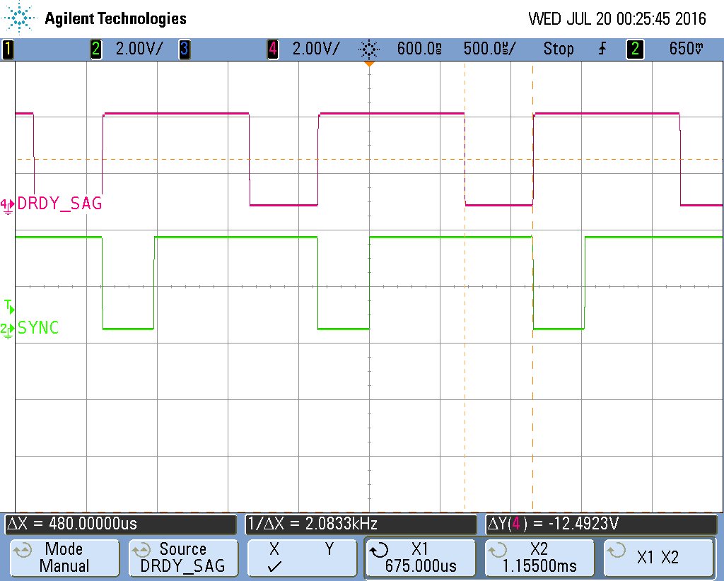
  • Figure 1 - Scope with SYNC and DRDY signals from ADS1255 ( for one shor reading in according to datasheet)

    Hi Chris

    Sure my friend.

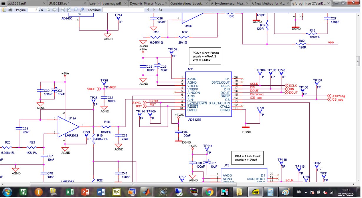
    I am attaching not only the schematic where I am using the ADS1255 but some screenshots from SYNC and DRDY signal to acquire samples in ine shot in according to datasheet.

    The bad news is that I am failing all the times to read the registers with RREG. I don't attempt to read the data register yet , since the most simple read is failling all the times

    The figure 1  shows the SYNC and DRDY signals , they are provided by a CPLD to keep t18 as closer as possible to datasheet (my measures points to 678 us).

    Figure 2 - ADS 1255


    The SYNC , CLKIN are provided by CPLD (specially the latest one to keep the clock signal as clean as possible).

    The DRDY signal is sent to LPC2132 ARM processor to be use as interrupt or to monitoring the SEFCAL procedures.

    We are using differential mode and in this case we can not connect AINCOM ( labeled AINCON).

    Please feel free to ask more information if you need .

    Once more thanks a lot for your support ,

    Shigueru

  • Hi Shigueru,

    Thanks for sharing your schematic!

    Do you need to synchronize the ADS1255 after each conversion?
    I would recommend leaving SYNC high and seeing if your issue goes away. The ADS1255 does not communicate over SPI while SYNC is low; also there is a very strict timing requirement for using the hardware SYNC:

    Best Regards,
    Chris

  • Hi Chris ,

    I did what you propose but unfortunatelly it didn't work as expected. 

    The read register operation is still failing yet.

    I am totally out of ideas or tips.  

    Thanks

    Shigueru

  • Hi Shigueru,

    I looked at your schematic again and noticed that you have separate analog and digital grounds. Do these connect together anywhere?
    If the grounds are not referenced to a common-potential, then the device will not function properly.

    Best Regards,
    Chris
  •  Hi Chris

    Yes they are connected together , just separated by a 10 ohms resistor ( see schematic )

    Thanks a lot

    Shigueru

  • Hi Shigueru,

    Hmm, 10-20 Ohms shouldn't cause communication issues, but it could degrade the ADC's noise performance (I would recommend shorting AGND and DGND together at the ADC, you want this to be a low-impedance connection). Are these ground connections physically far away from the ADC? If so, then you might have more impedance and a larger potential difference in these ground connections than you'd expect.

    I'm kind of running out of ideas myself, but...

    Have you looked at the RREG command sequence on the oscilloscope? Is the ADC really outputting all zeros (0x00) or could this be a code issue, where the code is just returning all zeros? I believe you only showed me a scope shot of your initialization sequence.

    Is the ADS1255 responding to other commands (outputting something other than zero)? It would be odd for the device to respond to some commands and not others, usually SPI communication works or it doesn't. If nothing is working than usually the problem is something like a missing supply or clock, or accidentally setting the nPWDN pin low. If you are seeing other responses from the device, than I might look into the "ssp_read_byte()" command to see if it is returning the correct data.

    Best Regards,
    Chris

  • Hi Chris

    This will be a long text , sorry for this, but I will try to give as much as detail as possible ( including some points that could give us some reason)

    First of all I measure with a 71/2 digits multimeter the potential betwen AGND and DGND and the vaule is 20mV.

    In case of RREG , all the times we get a zero value , but  we build another board and in the beggining the ADS1255 seems to work better reading data values , but after some attempts it stops and no return more.

    At this point I measure al maximum settings to see if any damage could be done and in the CLKIN the value was :

    f = 7.68MHz

    Maxumum Value = 4.096V

    Minimum Value = A peak with less than microseconds but around -0.6V ( in datasheet the value is -0.3V) . Could be a point ?

    To avoid confusion we call ths the new board and the other old board

    I didn't see it in old because there are another circuits like CPLD , DDS , Digital Potentiometers and we are testing one by one ,maybe the ADS couldbe affected by this.

    I will send you a screenshot of this value in this week.

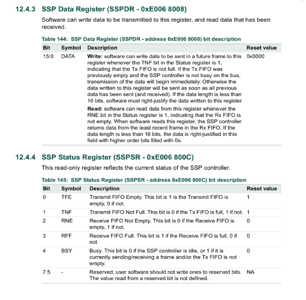
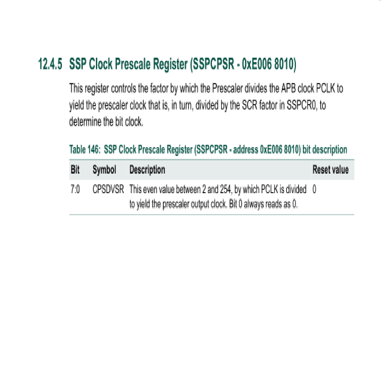
    About the SSP , I am attaching the user manual and bellow the code

    /******************************************************************************
    * Function : ssp_read_ads1255 *
    * In Parameter : None *
    * Out Parameter : None *
    * Description : Configure the SSP for ads1255 Register readings *
    *******************************************************************************/
    void ssp_read_ads1255(void)
    {
    SSPCR1 = 0x00;
    SSPCPSR = 48; // Set the SCLK to 0,96MHz
    SSPCR0 = 0x87; // SPI Mode 1 , 8 bits , SPI Frame Format
    SSPCR1 = 0x02; // SSP Master Mode is enabled

    /******************************************************************************
    * Function : ssp_send_byte *
    * In Parameter : unsigned char (byte) *
    * Out Parameter : unsigned char (byte) *
    * Description : Send byte over SSP *
    *******************************************************************************/
    void ssp_send_byte(u8 data)
    {

    /* Awaiting the FIFO to be empty */
    while (!(SSPSR & SSPSR_TFE));

    /* Send Data */
    SSPDR = data;

    /* Awaiting FIFO TX to be empty */
    while (!(SSPSR & SSPSR_TFE));

    /* Awating SSP to be available to start read*/
    while((SSPSR & SSPSR_BSY));

    }

    /*******************************************************************************
    * Function : ssp_read_byte *
    * In Parameter : None *
    * Out Parameter : unsigned char (byte) *
    * Description : Read byte over SSP *
    *******************************************************************************/
    u8 ssp_read_byte(void)
    {
    u16 data = 0;

    ssp_clean_rx_buffer();

    /* Awaiting the TX FIFO to be empty */
    //while (!(SSPSR & SSPSR_TFE));

    /* Writing Data on MOSI to generate the clock */
    SSPDR = 0; //dummy

    /* Awaiting the TX FIFO to be empty */
    while (!(SSPSR & SSPSR_TFE));

    /* Awaiting the SSP to be ready for starting reading */
    while((SSPSR & SSPSR_BSY));

    /* Awaiting a new incoming byte in Input FIFO */
    while(!(SSPSR & SSPSR_RNE));

    data = SSPDR; /* Reading the data*/

    return (u8)data;
    }

    Continue.....

    Thanks 

    Shigueru

  • And finally the Delay functions that I am using. 

    /******************************************************************************/
    /* Function Name : Delay1us */
    /* Description : Each tick is equivalent to 1us for MCLK = 46.08 MHz */
    /* Input Parameter: unsigned int (u32) */
    /* Output Parameter : NONE */
    /******************************************************************************/

    void Delay1us ( volatile u32 tempo )
    {
    volatile u8 loop;

    while ( tempo-- )
    {
    for ( loop = 0; loop <5 ; loop++ );
    }

    }

    /******************************************************************************/
    /* Function Name : DelayMs */
    /* Description : Each tick is equivalent to 1ms for MCLK = 46.08 MHz */
    /* Input Parameter: unsigned int (u32) */
    /* Output Parameter : NONE */
    /******************************************************************************/
    void DelayMs ( u32 tempo )
    {
    u16 loop;

    while ( tempo-- )
    {
    for ( loop = 0; loop <8000 ; loop++ );
    }

    }

    Thanks

    Shigueru

  • One more info about SSP

    Thanks

    Shigueru

  • Hi Shigueru,

    Shigueru Nagao said:

    At this point I measure al maximum settings to see if any damage could be done and in the CLKIN the value was :

    f = 7.68MHz

    Maxumum Value = 4.096V

    Minimum Value = A peak with less than microseconds but around -0.6V ( in datasheet the value is -0.3V) . Could be a point ?

    It is hard to say, any thing outside of the absolute maximum ratings has the potential to damage the device. If it is only slightly outside of spec it may only degrade the lifetime of the device. However, I would be concerned that your scope only showed a bandwidth-limited signal, in which case, the peak amplitude may have been larger.

    Why is the clock 4.096V, instead of 3.3V (DVDD)? Is your LPC2132 Processor operating off of 5V logic?
    If so, then perhaps the 3.3V output is not above the logic-high threshold of the processor. Perhaps the old device was outputting a slight larger voltage on DOUT and your processor was reading it correctly. What do you think?

    I'm not familiar with the LPC2132 Processor, but it looks like your read SPI function is checking for the correct flags to indicate that data was sent and received. If you've read data correctly before, then likely the issue isn't with this code.

    Best Regards,
    Chris

  • Hi Chris,

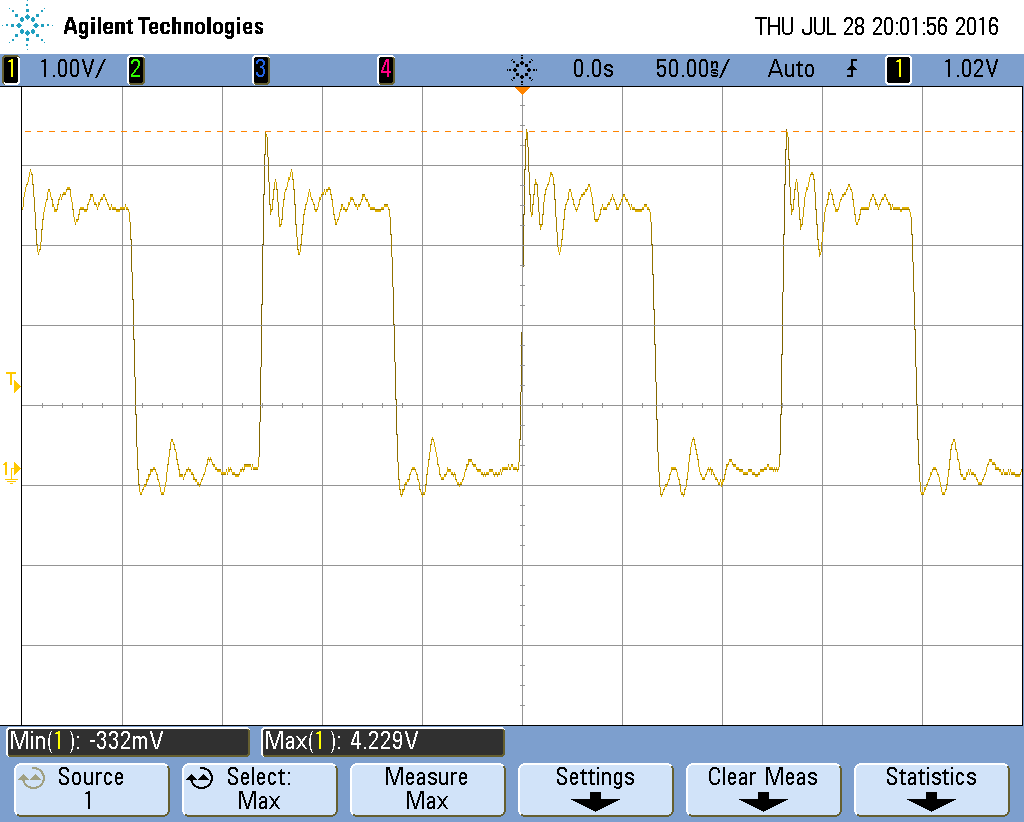
    Your points are correct . The CLKIN is supplied by a CPLD and it is powered by 3.3V . I have a look once more in datasheet and the section related to CLOCK GENERATION is telling to keep clock as  a clean waveform , in the picture attached you will see this waveform and it is not a clean in my point of view. There are some overshoots and undershoots.

    Do you have any idea about how to fix it ( resistors , capacitors) ?

    Another point in the application it is mentioning something about 100 ohms resistor  in CS SCLK and other digital pins. In my board they are missing  ( I don't know why , since I am not the board designer). Does it could be the reason ( or at least one fo the reasons) ?

    Thanks

    Shigueru

  • Hi Chris

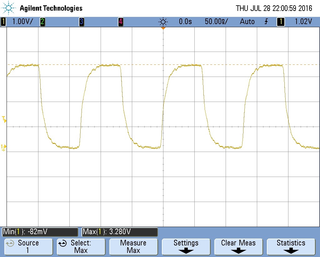
    We put a 270R resistor in serie in CLK line. The new waveform looks like this.

    Thanks 

    Shigueru

  • Hi Shigueru,

    That looks much cleaner! Is that having any effect on the SPI communication?

    Also, is your processor on the same board as the ADS1255, or are you jumper wiring two boards together?
    If jumper wiring, try to keep the wires short and don't forget to connect the grounds together. I'll usually wrap the SPI signal wires around the ground wire to minimize the loop area (i.e. added inductance) to the wires.

    Best Regards,
    Chris

  • Hi Chris

    They are in the same board.
    We have a good news is that the behavior is much more stable. We are getting some values
    We are almost there my friend. I will keep you updated.

    Thanks
    Shigueru
  • Hi Shigueru,

    Good news finally!

    Please let me know what else I can do to help.

    Best Regards,
    Chris