This thread has been locked.

If you have a related question, please click the "Ask a related question" button in the top right corner. The newly created question will be automatically linked to this question.

ADS1248 3 Channel Multiplexing following example

Other Parts Discussed in Thread: MSP430F5438, ADS1248, ADS1246

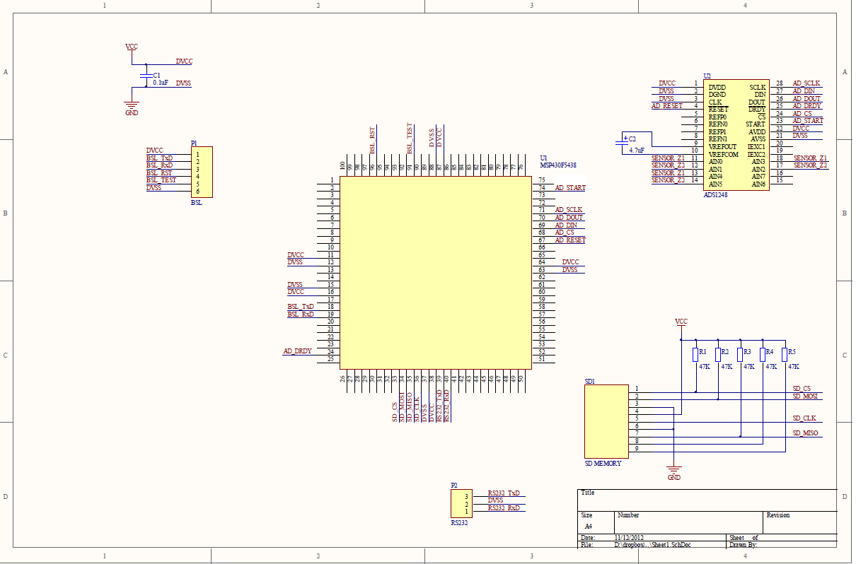
Hello, I'm trying to run an ADS1248 following the example on page 55 of the device datasheet. The only difference is that I'm doing it with 3 channels. I'm trying to do this with a MSP430F5438. I attach a picture with the schematic. I know that it isn't a hardware problem, because I run it with different configurations, but this is the configuration I need for my application. 

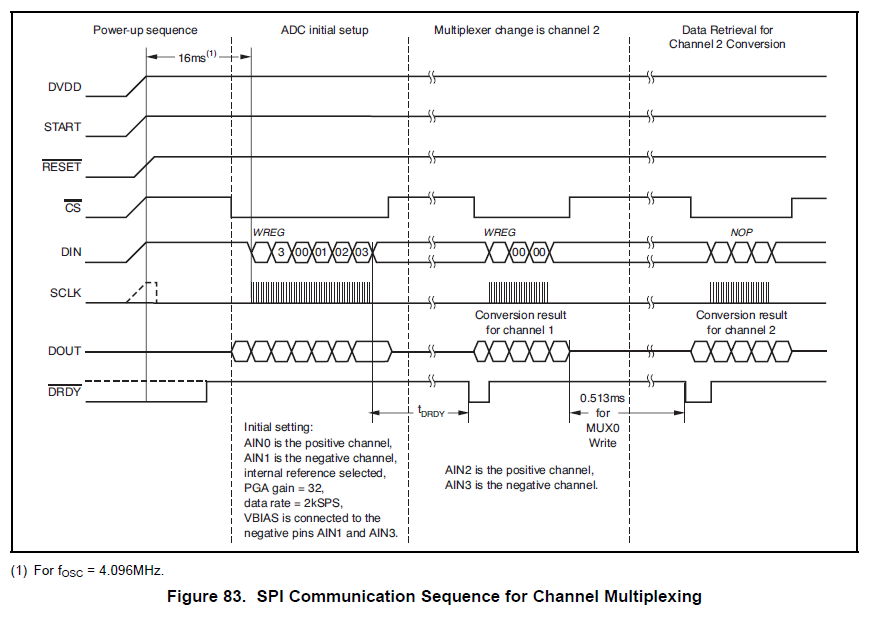
First of all, I make the initialization of the MSP, initializing the  LFXT1 at 8MHz and the series port. Then I start my code following the Figure 83 of the ADS1248 datasheet (Figure 83. SPI Communication Sequence for Channel Multiplexing). 

I'm going to explain my code, because I think that I'm making a mistake in the process.

First off all, I make an initialization of the SPI that communicates with the AD. I put a frequency of 1MHz. I also configure the port P1,7 as a  Lo/Hi interrupt. I put the Sart, Cs and Reset pins at high value (CS and reset are active at low state, so I put a 0 on them). Then I make a delay of 2^16 cycles and then I put the CS on low state. 

After this, I start the configuration of the registers of the AD.

First of all, I send the WREG command, 0100 0000 indicating that the address of the first register to read is 0. Then I read and discard the answer of the AD. Then I send an 0B, indicating that I'm going to write in 12 registers. I continue sending the values of the registers and reading the answer of the AD. When this finishes I put the CS to high state. 

Then in the main program I wait until DRDY goes from Lo/Hi, when this happens I put the CS to low state and I start reading and discarding the first value. Then I send WREG in order to indicate that I want to change the channel I'm using . I use the first to sends to send the WREG values. Meanwhile I save the first two values of the conversion (MSB and the middle value). Then I send the value of the following channel (If I had read CH0, now I say that I want CH1, if I'm in CH1, I say CH2, and if I'm in CH2 I return to CH0). After saing the value of the register MUX0 I read the LSB of the conversion. Then I put the CS to high state and I returnto wait the DRDY signal.

Sorry if there is any spelling mistake. Can somebody help me with this? If it is necessary I can put my code here. 

Also a Code of the implementation on this diagram with some MSP can be very helpful for my project.

Best regards.

  • Hi Santiago,

    It would be helpful to look at your code. Below is pseudo code describing how I would accomplish what you're trying to do. Below I'm assuming you're writting full duplex; writing registers while reading results. I'm also going to use the RDATAC command, which automatically loads a completed result to the output shift register on the falling edge of each DRDYn. I wasn't able to immediately discern what problem you're seeing, but one thing that I did not notice was the inclusion of the RDATA or RDATAC command. These commands are used to configure the output shift register to load the result. Without issuing one or the other of these commands, you wont be able to read conversion data from the ADS1248.

    Power Up:
    START: 1
    RESETn: 1
    CSn: 1
    DIN: 1
    SCLK: 0

    Wait 2^16clk (16ms for internal oscillator)

    Issue RDATAC command to allow results to load into output register:
    START: 1
    RESETn: 1
    CSn: 0
    SCLK: X
    DIN: 14h //Can be idled high or low if using dedicated DRDY pin
    DOUT: Ignore

    Configure channel CH0 AIN0:AIN1: // Can immediately follow the RDATAC command without needing to frame CSn
    START: 1
    RESETn: 1
    CSn: 0
    SCLK: X
    DIN: 40h 0Bh 01h XXh XXh XXh XXh XXh XXh XXh XXh XXh XXh XXh
    DOUT: Ignore
    Raise CSn at end if needed

    Wait for falling edge of DRDYn

    Configure channel CH1 AIN2:AIN3 and read CH0 data:
    START: 1
    RESETn: 1
    CSn: 0
    SCLK: X
    DIN: 40h 0Bh 13h XXh XXh XXh XXh XXh XXh XXh XXh XXh XXh XXh
    DOUT: XXh(MSB) XXh XXh(LSB) //Results from CH0 reading. Can be read at the same time 40h 0Bh 13h are written (full duplex).
    Raise CSn at end if needed

    Wait for falling edge of DRDYn

    Configure channel CH2 AIN4:AIN5 and read CH1 data:
    START: 1
    RESETn: 1
    CSn: 0
    SCLK: X
    DIN: 40h 0Bh 25h XXh XXh XXh XXh XXh XXh XXh XXh XXh XXh XXh
    DOUT: XXh(MSB) XXh XXh(LSB) //Results from CH1 reading. Can be read at the same time 40h 0Bh 25h are written (full duplex).
    Raise CSn at end if needed

    Wait for falling edge of DRDYn

    Configure channel CH0 AIN0:AIN1 and read CH2 data:
    START: 1
    RESETn: 1
    CSn: 0
    SCLK: X
    DIN: 40h 0Bh 01h XXh XXh XXh XXh XXh XXh XXh XXh XXh XXh XXh
    DOUT: XXh(MSB) XXh XXh(LSB) //Results from CH2 reading. Can be read at the same time 40h 0Bh 01h are written (full duplex).
    Raise CSn at end if needed

    Repeat Configure channel CH1 AIN2:AIN3 and read CH0 data step

    Best regards,
    Mike Beckman
    Delta Sigma ADC Product Line Manager

  • Hello Mike, this is the my code adapted with your specifications. I put as an input a sinusoidal signal of 10Hz , 1Vpp and 1V of offset. I'm trying to see it in a labview program that I have make but it isn't working. I put here algo the vi.

    Best regards.

    Santi

    /*
     * main.c
     */
    
    #include "msp430x54x.h"
    #include "ads1248.h"
    #include "puerto_serie.h"
    #include <stdio.h>
    #include <string.h>
    
    
    int i,OK;
    unsigned char dummy;
    unsigned char valor[3];
    unsigned char channel[3] = {0x01,0x13,0x25};
    
    void ADS1248AssertCS(int fAssert)
    {
       if (fAssert)
          P9OUT &= ~(ADS1248_CS);
       else
          P9OUT |=  ADS1248_CS;
    }
    
    int initSPIads1248(void)
    {
      //Configuraci�n del puerto 9:
      //P9.1 UCB2SIMO -> Salida del master
      //P9.2 UCB2SOMI -> Entrada del master
      //P9.3 UCB2CLK -> Clock
      //P9.0 O -> ADS1248_CS, se activa a nivel bajo
      //P9.6 O -> ADS1248_START
      //P1.7 I <- ADS1248_DRDY, ACTIVAMOS LA IRQ DEL PUERTO 1.7
    
      P9DIR &= 0x30;
      P9DIR |= 0x41;
      P9SEL &= 0x30;
      P9SEL |= 0x0E;
    
      P1DIR &= 0x7F;
      P1DIR |= 0x00;
      P1SEL &= 0x7F;
      P1SEL |= 0x00;
      P1IE |= 0x80;                             // P1.7 interrupt enabled
      P1IES |= 0x80;                            // P1.7 Hi/Lo edge
      P1IFG &= ~0x80;                           // P1.7 IFG cleared
    
      //P8.6 O -> ADS1248_RESET, se activa a nivel bajo
      P8SEL &= 0x00;
      P8DIR &= 0x00;
      P8DIR |= 0x40;
    
      //PROBANDO
      UCB2CTL1 |= UCSWRST;
    
      //Definimos el registro de control: 8 bit, Modo Master, MSB se recibe primero, Modo Sincronico
      UCB2CTL0 |= UCMST + UCMSB + UCSYNC/* + UCCKPL*/;
      //Definimos el segundo registro de control: Fuente de Reloj SMCLK
      UCB2CTL1 |= UCSSEL_2;  // SMCLK
      //Pre-escalamos el Clk a SMCLK/8 = 8Mhz/8
      UCB2BR0 = 0x08; // /8 SMCLK/8 = 8Mhz/8 = 1MHz
      UCB2BR1 = 0;    //
      //UCB0MCTL = 0;  // No modulation
      //Habilitamos para que funcione el Modulo de Comunicacion
      UCB2CTL1 &= ~UCSWRST; // **Initialize USCI state machine**
    
      /*
      //LO AGREGAMOS PARA HABILITAR LA INTERRUPCION
      UCB2IE |= UCRXIE;                         // Enable USCI_B2 RX interrupt
       */
    
      return 0;
    }
    
    void init(void)
    {
    	WDTCTL = WDTPW + WDTHOLD;				// Stop WDT
    	
    	// Initialize LFXT1
    	P7SEL |= 0x03;                            // Select XT1
    	UCSCTL6 &= ~(XT1OFF);                     // XT1 On
    	UCSCTL6 |= XCAP_3;                        // Internal load cap C=12.0pF
    
    	// Loop until XT1 fault flag is cleared
    	do
    	{
    	  UCSCTL7 &= ~XT1LFOFFG;                  // Clear XT1 fault flags
    	}while (UCSCTL7&XT1LFOFFG);               // Test XT1 fault flag
    
    	// Initialize DCO to 2.45MHz
    	__bis_SR_register(SCG0);                  // Disable the FLL control loop
    	UCSCTL0 = 0x0000;                         // Set lowest possible DCOx, MODx
    	UCSCTL1 = DCORSEL_6;                      // Set RSELx for DCO = 4.9 MHz
    	UCSCTL2 = FLLD_1 + 243;                   // Set DCO Multiplier for 2.45MHz
    	                                          // (N + 1) * FLLRef = Fdco
    	                                          // (243 + 1) * 32768 = ___ MHz
    
    	                                          // Set FLL Div = fDCOCLK/2
    	__bic_SR_register(SCG0);                  // Enable the FLL control loop
    
    	  // Worst-case settling time for the DCO when the DCO range bits have been
    	  // changed is n x 32 x 32 x f_MCLK / f_FLL_reference. See UCS chapter in 5xx
    	  // UG for optimization.
    	  // 32 x 32 x 8 MHz / 32,768 Hz = 249856 = MCLK cycles for DCO to settle
    	__delay_cycles(64000);
    	__delay_cycles(64000);
    	__delay_cycles(64000);
    	__delay_cycles(64000);
    
    }
    
    
    void initRS232(void)
    {
    	P3SEL = 0x30;                           // P3.4,5 = USCI_A0 TXD/RXD
    
    	UCA0CTL1 |= UCSWRST;                      // **Put state machine in reset**
    	UCA0CTL1 |= UCSSEL_2;                     // CLK = DCO
    
    	UCA0BR0 = 0x41;                           // ~8MHz/9600=833 (see User's Guide)
    	UCA0BR1 = 0x03;                           //
    	//UCA0MCTL = UCBRS_2+UCBRF_0;               // Modulation UCBRSx=2, UCBRFx=0
    	UCA0CTL1 &= ~UCSWRST;                     // **Initialize USCI state machine**
    	//UCA0IE |= UCRXIE;                         // Enable USCI_A0 RX interrupt
    }
    
    void enviaRS232(unsigned char Code)
    {
    	while (!(UCA0IFG&UCTXIFG));             // USCI_A0 TX buffer ready?
    	UCA0TXBUF = Code;
    }
    
    
    void main(void)
    {
    
    	OK=0;
    	i=0;
    
    	init();
    	initRS232();
    	initSPIads1248();
    
    	//ADS1248 Power UP
    	/************************/
    	P9OUT |= ADS1248_START; 			//Start High
    	P8OUT |= ADS1248_RESET; 			//Reset High
    	ADS1248AssertCS(0);					//CS goes high
    	while (!(UCB2IFG&UCTXIFG));			//DIN = 1
    	UCB2TXBUF = 0x01;
    	while (!(UCB2IFG&UCRXIFG));			//I ignore DOUT
    	dummy=UCB2RXBUF;
    	__delay_cycles(64000);
    	__delay_cycles(1536);				//Delay of 2^16cycles = 8Mhz*65536 = 8ms
    	/************************/
    
    	//Issue RDATAC command to allow results to load into output register
    	/************************/
    	ADS1248AssertCS(1);					//CS goes low
    	while (!(UCB2IFG&UCTXIFG));			//DIN = RDATAC command
    	UCB2TXBUF = 0x14;
    	while (!(UCB2IFG&UCRXIFG));			//I ignore DOUT
    	dummy=UCB2RXBUF;
    	/************************/
    
    	//Configure channel CH0 AIN0:AIN1
    	/************************/
    	while (!(UCB2IFG&UCTXIFG));			//Write Register
    	UCB2TXBUF = 0x40;					//0100 nnnn -> Direcci�n del primer registro a esbribir
    	while (!(UCB2IFG&UCRXIFG));
    	dummy=UCB2RXBUF;
    	while (!(UCB2IFG&UCTXIFG));
    	UCB2TXBUF = 0x0B;					//0000 nnnn -> n� de bytes a escribir - 1
    	while (!(UCB2IFG&UCRXIFG));
    	dummy=UCB2RXBUF;
    	while (!(UCB2IFG&UCTXIFG));
    	UCB2TXBUF = 0x01;					//MUX0  -> 00(Burnout current off)000(AIN0 as positive channel)001(AIN1 as negative channel)= 0000 0001
    	while (!(UCB2IFG&UCRXIFG));
    	dummy=UCB2RXBUF;
    	while (!(UCB2IFG&UCTXIFG));
    	UCB2TXBUF = 0x00;					//VBIAS -> 0, VBIAS not enabled
    	while (!(UCB2IFG&UCRXIFG));
    	dummy=UCB2RXBUF;
    	while (!(UCB2IFG&UCTXIFG));
    	UCB2TXBUF = 0x30;					//MUX1 -> 0 (Internal Oscilator) 01 (Internal reference always ON (necessary to use IDAC)) 10 (On board reference selected (Before 00 by defect)) 000 (Normal operation) 0011 0000
    	while (!(UCB2IFG&UCRXIFG));
    	dummy=UCB2RXBUF;
    	while (!(UCB2IFG&UCTXIFG));
    	UCB2TXBUF = 0x05;					//SYS0 -> 0 (por defecto) 000 (PGA=1) 0101 (160 SPS) = 0000 0101
    	while (!(UCB2IFG&UCRXIFG));
    	dummy=UCB2RXBUF;
    	while (!(UCB2IFG&UCTXIFG)); 		//Offset calibration coefficient register, lo dejamos a =, por lo tanto una salida de 0 es equivalente a 0V
    	UCB2TXBUF = 0x00;					//OFC0
    	while (!(UCB2IFG&UCRXIFG));
    	dummy=UCB2RXBUF;
    	while (!(UCB2IFG&UCTXIFG));
    	UCB2TXBUF = 0x00;					//OFC1
    	while (!(UCB2IFG&UCRXIFG));
    	dummy=UCB2RXBUF;
    	while (!(UCB2IFG&UCTXIFG));
    	UCB2TXBUF = 0x00;					//OFC2
    	while (!(UCB2IFG&UCRXIFG));
    	dummy=UCB2RXBUF;
    	while (!(UCB2IFG&UCTXIFG));			//Full-scale calibration coefficient register, para un PGA = 1, ha de ser 0100 0000 0000 0000 0000 0000 = 0x400000
    	UCB2TXBUF = 0x00;					//FSC0
    	while (!(UCB2IFG&UCRXIFG));
    	dummy=UCB2RXBUF;
    	while (!(UCB2IFG&UCTXIFG));
    	UCB2TXBUF = 0x00;					//FSC1
    	while (!(UCB2IFG&UCRXIFG));
    	dummy=UCB2RXBUF;
    	while (!(UCB2IFG&UCTXIFG));
    	UCB2TXBUF = 0x40;					//FSC2
    	while (!(UCB2IFG&UCRXIFG));
    	dummy=UCB2RXBUF;
    	while (!(UCB2IFG&UCTXIFG));
    	UCB2TXBUF = 0x00;					//IDAC0 -> xxxx (solo lectura) 0 (DOUT/DRDY solo como salida de datos) 000 (fuente de corriente decoenctada) = 0x00
    	while (!(UCB2IFG&UCRXIFG));
    	dummy=UCB2RXBUF;
    	while (!(UCB2IFG&UCTXIFG));
    	UCB2TXBUF = 0xCC;					//IDAC1 -> 11xx 11xx (desconectadas) = 0xCC
    	while (!(UCB2IFG&UCRXIFG));
    	dummy=UCB2RXBUF;
    	/************************/
    
    	ADS1248AssertCS(0);					//CS goes high
    	__bis_SR_register(GIE);				//Activo las Interrupciones
    
    	while(1)
    	{
    		while(OK==0);					//Wait for falling edge of DRDYn
    
    		while (!(UCB2IFG&UCTXIFG));
    		UCB2TXBUF = 0x40;				//WREG 1 (0x40 -> el 0 corresponde a la direcci�n del primer Reg a escribir MUX0)
    		while (!(UCB2IFG&UCRXIFG));
    		valor[0]=UCB2RXBUF;				//MSB
    		while (!(UCB2IFG&UCTXIFG));
    		UCB2TXBUF = 0x40;				//WREG 2 (0x00 -> el 0 corresponde a que se escribir� 1 byte -1)
    		while (!(UCB2IFG&UCRXIFG));
    		valor[1]=UCB2RXBUF;				//2� data
    		while (!(UCB2IFG&UCTXIFG));
    		UCB2TXBUF = channel[i];			//Valor del registro MUX 0, ser� el siguiente canal
    		while (!(UCB2IFG&UCRXIFG));
    		valor[2]=UCB2RXBUF;				//LSB
    
    		ADS1248AssertCS(0);					//CS goes high
    
    		//Envio el resultado de la conversi�n por puerto serie
    		enviaRS232(valor[0]);
    		enviaRS232(valor[1]);
    		enviaRS232(valor[2]);
    	}
    }


    // Port 1 interrupt service routine
    #pragma vector=PORT1_VECTOR
    __interrupt void Port_1(void)
    {
    	OK=1; 						//Pongo el OK a 1 para poder continuar en el programa principal
    	if (i==2){					//Cambiamos el valor del entero del vector que cambia de canal
    		i=0;
    	}
    	else{
    		i++;
    	}
    	ADS1248AssertCS(1);			//CS goes LOW
    	P1IFG &= ~0x80;				// P1.7 IFG cleared
    
    }

    1374.prueba 3 chanels.rar

  • Santi,

    I noticed on line 238 of your c-code you write the following:

    UCB2TXBUF = 0x40; //WREG 2 (0x00 -> el 0 corresponde a que se escribirá 1 byte -1)

    You wrote 0x00 in your comments, which is correct. The 0x40 will keep the ADC from writing to the MUX0 register. It's actually setting the internal state machine back to the WREG command so the next command UCB2TXBUF = channel[i] is actually telling the ADS1248 how many registers to write to.

    I didn't notice any other errors in your communication with the ADS1248. Are you getting any DRDYn pulses out of the device? A quick way to check would be to grab an oscilloscope and trigger on the DRDYn pin to see if you're issuing the commands. If the pulses are spaced 63ms apart then you've initialized  the device correctly.

    Regards,
    Mike 

  • Finally the program is working, I had forgotten to put the OK variable to 0. 

    Now I have a pair f doubts: When I configure the ADS1248 at 160SPS, how does it work? I mean, I will be able to see a sinusoidal waveform of 16Hz (10 points per period) in the three channels? Or the SPS will be divided by the numbers of channels I have?

    Another doubt, if I increase the master clock with an external crystal to 20MHz, I will have more or less time between DRDY's falls?

    Best regards

  • Santiago,

    As there is only one ADC, you will have to split the data rate by the number of channels being measured.  There may be additional time required based on the actual time it takes to switch the mux and reset of the digital filter.  For three channels at 160sps, your effective sampling per channel is about 50Hz.

    The nominal frequency is 4.096MHz, and the maximum clock that can be applied to the ADS1248 is 4.5MHz (so you can't use 20MHz.)  Increasing the fclk will shorten the time between DRDY pulses, or another way to look at it is the data rate increases.  Table 16 of the datasheet shows the number of clock cycles per data rate.  For 160sps nominal the actual time for a 4.096MHz clock is actually 160.602sps.  It changes to 176.443sps for 4.5MHz.

    Best regards,

    Bob B


  • There is one thing I don't understand about the clock source. We have 2 pins, the CLK and the SCLK pins. I have connected the CLK pin to GND, so the internal oscillator is  activated, and I have the SCLK pin connected to the clock source of the UCB2CLK SPI. 

    My master clock (the one that provides the MSP) is 8MHz, but the UCB2CLK is pre escalating like this: SMCLK/8 = 8Mhz/8 =1MHz. This should be 4MHz? What is the goal of using or not the CLK pin??

    Best regards

  • Santiago,

    The CLK pin allows for an external clock input.  This allows for some clock scaling or for a more precise clock than what is available on the ADS1248.  This CLK is used as the device master clock which establishes the modulator rate among other things.  When the pin is grounded, the internal clock is used.

    The SCLK is strictly for communication and only runs when communicating.  The maximum SCLK speed can be no faster than 2MHz, but can run much slower.  1MHz is fine.

    Best regards,

    Bob B

  • Thanks you very much, you are helping me a lot. 

    I`m going to change my application and my hardware because I need the lecture oof the three channels at the same time. So I'm going to use 3 ads1246. Is there any configuration (using RDATAC) where isn't necesary to give a data in to the ad to read the result? I mean, when a data is ready, the DRDY pin goes low and I Can read the data without sending anything.

    Best regards

  • Santiago,

    Using the internal oscillator can be somewhat problematic as you will not know exactly when the data will be completed by each of the ADS1246s.  You could issue a SYNC to have them all start converting at the same time, but they could still be running at slightly different data rates.

    The best way is to use an external oscillator clock source where all three devices are running at the same rate.  In this way you only have to monitor one DRDY, and then the data will be available at the same time.  If you use RDATAC, then all you have to do is read out the 3 bytes of data.  You do not have to issue a command.

    The process would be to wait for DRDY to go low, then read one device at a time until all data is read.  You can use one SPI bus, but you will need to have three separate CS lines.  You may also want to have a GPIO line connected to SYNC pins so you can control the actual conversion start time if you write to the registers.

    Best regards,

    Bob B

  • HI Bob, now my 3 ADS1246 have arrived and I have connected them. I have connected both CLKs pins to an ACLK output configured to 4MHz. The other connections are similar to the connections I had made for the ADS1248 (when I have it, if it is necessary, I'll put an schematic).

    Now my doubt. What is the correct way to proceed in the configuration? I mean, when I worked with the ADS1248 I first did a "power up" (START and RESET high, CS low), then I send a RDATAC command, then I configured all the registers and finally I start to read, waiting the DRDY to go low. Now I want a good synchronisation between the 3 ADS1246. Can I change the order? I mean, fist of all, registers configurations, second RDATAC command, and finally, "power up" and start to wait for one DRDY to go low.

    Best regards,

    Santi

  • Hi Santiago,

    To write to the registers START must be high.  You can follow the same procedure except for after the last device configuration you pull START low, and wait for DRDY to transition from high to low.  At this point all devices will be in the power down state.  Returning START high will resynchronize them and they should be converting at the same time.

    Best regards,

    Bob B