This thread has been locked.

If you have a related question, please click the "Ask a related question" button in the top right corner. The newly created question will be automatically linked to this question.

ADS 7823 Comm Issues

Other Parts Discussed in Thread: ADS7823

I am getting a weird behavior from reading the ADS 7823. Instead of returning the value on a a read it gives back its own address in the first byte and 11111111 for the remaining 7 bytes.

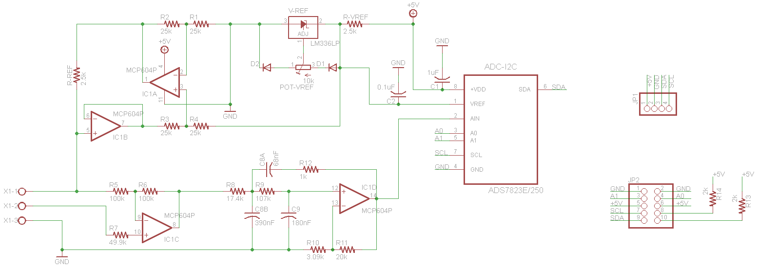
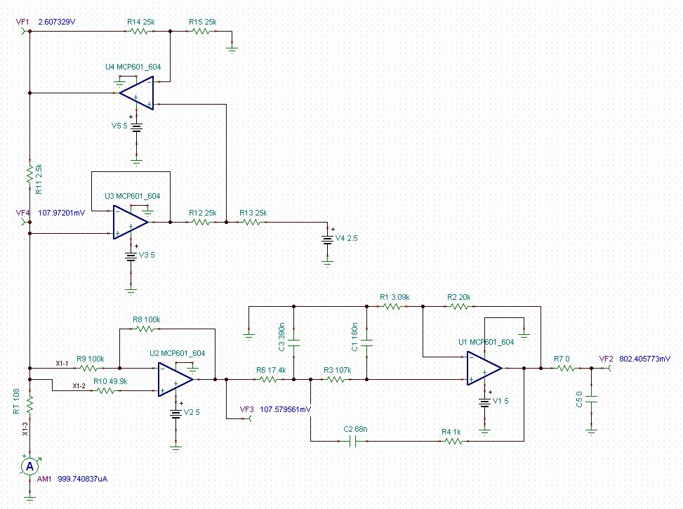
The circuit is on a fab'd PCB that I designed. The supply is +5V for the whole circuit. I connect to the board with a PIC and trying to read in 4 samples as the ADS 7823 supplies over I2C. I have 2k ohm pull-up resistors on each SDA and SLC lines. It takes a 3 wire RTD, converts it to voltage, amplifies it to a 0-2.5V scale and hands that to the ADS 7823 analog input. The reference voltage is supplied by a tuned lm336-2.5. I have two boards constructed so far and tested. I incorporated test points and all my analog signals are fine: steady and accurate.

On the first board I have never seen a good value come through. All I get is address back as mentioned before. I tried changing the address from both to ground to both to supply and it didn't report anything back. I haven't tried that board since. I had solder bridging the ADC's pins 5-8 when I first reflowed it, so I used an iron and wicked it away. I tried a second PIC and had the same issue.  I thought I may have overheated it and tried the second board I built.

The second board had one bridge between v-ref and v-in that I quickly wicked away. This board actually reported back values on all 4 sample per read at first for at least 40 reads. I tried it again later and it didn't work. It started doing the same thing as the other: giving back its address and 7 maxed bytes.

I don't have a scope which makes this a pain. I checked continuity before and after soldering. All the voltages are right. The program is simple, writes the address, writes the command, reads in 8 bytes, serial out to my PC and loops. I am at a loss for what is wrong.

  • Hi Chris,

    A few questions:

    - What voltages are you applying at X1-1 and X1-2?

    - What SCL frequency are you using? Are you using I2C in HS mode? (as described in fig. 4)

    - Can you please send me your source code showing how you initiate an ADC conversion and read back the results?

    Also, can you try decreasing the ADC's supply voltage to 3.5V and let me know if your results change?

    Thanks,

    Harsha

  • X1-1 provides 100 ohms at 0C and about 140 ohms at 100C. When I ran it the value was around 108 ohms. There is 1mV coming across Rref. X1-2 is used to measure resistance against to correct for distance errors (lines are the same length). The output at pin 8 of IC1C is 1mV per 1ohm from the sensor: 108 mV when I tested it.

    I ran this at both slow and fast: 100kHz and 400kHz respectively. I have tried so many combinations since it failed that I don't recall what speed it was set to when it worked, but I believe it was at 400kHz.

    My source code is skewed because I am prototyping with a PICAXE and it encapsulates the I2C commands. Once the HI2SETUP is defined the hi2cout and hi2cin automatically send the address first and changes the LSB according to the read/write mode. They also automatically send the acknowledge bit. The final project will be read from a different chip that is more I2C configurable. 

    _________________________________________

    HI2CSETUP I2CMASTER, %10010000, i2cfast, i2cbyte
    '----------------------- Main program cycle
    main:

    hi2cout (%00000000)
    hi2cin (b1,b0,b3,b2,b5,b4,b7,b6)
    sertxd ("Read1 is ",#Read1,CR,LF) ' Display A/D value
    sertxd ("Read2 is ",#Read2,CR,LF) ' Display A/D value
    sertxd ("Read3 is ",#Read3,CR,LF) ' Display A/D value
    sertxd ("Read4 is ",#Read4,CR,LF,CR,LF) ' Display A/D value
    pause 1000
    goto main
    _____________________________________________________

    I am not clear about about the fifth bit in the command byte so I have tried both 00001000 and 00000000. Neither work.

     My final project has a 3.3V supply built in, but the LM336-2.5 wont provide 2.5V with that low of supply. I still tried at 3.3, but i had the same result.

    Is there any reason why I would get the address back as the first byte?

  • OK, I follow the HS mode now. I didn't initialize it properly, but it doesn't matter because I am limited to 400 kHz anyway.

  • I have tried to run the board from the chip I intend to use ultimately without any luck. I tried at 5V and 3.3V. I tried 4k7 instead of the 2k ohm pull-up resistors without luck still. This is the code I used, but all I get are zeros now.


    func getADC(var i)

    var s,r,h1,l1,h2,l2,h3,l3,h4,l4;

    r := ADCI2C+i;

    I2C_Start(); // Generate Start condition
    print("Started\n");
    s:=I2C_Write(r);
    I2C_Nack();
    print("Ackd Address ",s," - ",r,"\n");

    s:=I2C_Write(0);
    I2C_Nack();
    print("Ackd Command ",s,"\n");

    I2C_Restart();
    print("Restarted\n");

    s:=I2C_Write(r+WR);
    I2C_Nack();
    print("Ackd Read ",s,"\n");

    h1 := I2C_Read();
    I2C_Ack();
    l1 := I2C_Read();
    I2C_Ack();
    h2 := I2C_Read();
    I2C_Ack();
    l2 := I2C_Read();
    I2C_Ack();
    h3 := I2C_Read();
    I2C_Ack();
    l3 := I2C_Read();
    I2C_Ack();
    h4 := I2C_Read();
    I2C_Ack();
    l4 := I2C_Read();
    I2C_Nack();
    print("Nackd\n");

    I2C_Stop(); // Send Stop Condition
    print("Stopped\n");


    r1 := (h1 << 8)+l1;
    r2 := (h2 << 8)+l2;
    r3 := (h3 << 8)+l3;
    r4 := (h4 << 8)+l4;


    endfunc


  • Chris,

    Sorry I couldn't respond earlier. I've been trying to eliminate possible design issues with your analog input circuitry that could cause the issue you are observing.

    My first suspicion is that your VREF input is not stable during ADC conversion. The load current drawn by the ADC from the reference input fluctuates greatly (datasheet specifies 9uA average over 8uS conversion period) and quickly as the ADC performs a conversion. Really the only way to meet these large load current demands quickly is to place a large capacitor on the VREF input close to the chip. Your circuit has C2 = 0.1uF to serve this purpose, which should technically keep VREF stable enough (limit the variation to <750uV or about 1.3LSB). However, could you please probe the VREF input of the ADC with a multimeter while the ADC is converting and let me know how much variation you are seeing? You can also try increasing C2 to 0.47uF.

    Also, attached is a DC simulation of the input circuit. I have used a 108ohm RTD resistance and an ideal 2.5V source in place of your reference source. Can you please verify that you are measuring all the same values on your board?

    We can shift focus to software if the hardware checks out.

    Best Regards,
    Harsha

  • My multimeter only goes down to 1mV resolution at 2.5V, but I have noticed a possible swing. Occasionally, I do see a 1mV drop around conversion. I have a 0.47uF cap on order to try it out.

    As for the values in your drawing, mine are right in line. At time of testing my RT resistance was a bit higher, but all values scaled were within 0.013 std dev.

    Point Actual Compared
    VF1 2.67 2.607329 0.976528
    VF2 829 802.405773 0.96792
    VF3 112 107.579561 0.960532
    VF4 112.2 107.97201 0.962317
    RTD Ohm 108.8 108 0.992647
    Std Dev -0.01312
  • Update:

    I have 0.47uF caps on order, but they haven't arrived, yet. I realized I had a spare 0.39uF on hand and tried that in place of the 0.1uF at C2. It seemed to do the trick and I am getting output from the ADC now using the PIC. Very smooth, no erratic readings at all. I will switch out the remaining C2 caps on the rest of my boards when the new caps arrive.

    However, I am using the 2nd program above on another chip (PICASSO from 4D labs) for final implementation, but it is not reading in values. I continue to get all zeros. I wrote it specifically based on the ADS7823 datasheet. The one possibility that I recognize could be an issue is the use of the NACK function after the WRITE function. I do this because the datasheet says I need another pulse after the write to trigger the ADS7823 to send an ACK. The NACK function releases the SDA high then pulses the clock, so I thought it would work fine. Any help or insight would be appreciated.


    func getADC(var i)

    var s,r,h1,l1,h2,l2,h3,l3,h4,l4;

    r := ADCI2C+i;

    I2C_Start(); // Generate Start condition
    print("Started\n");
    s:=I2C_Write(r);
    I2C_Nack();
    print("Ackd Address ",s," - ",r,"\n");

    s:=I2C_Write(0);
    I2C_Nack();
    print("Ackd Command ",s,"\n");

    I2C_Restart();
    print("Restarted\n");

    s:=I2C_Write(r+WR);
    I2C_Nack();
    print("Ackd Read ",s,"\n");

    h1 := I2C_Read();
    I2C_Ack();
    l1 := I2C_Read();
    I2C_Ack();
    h2 := I2C_Read();
    I2C_Ack();
    l2 := I2C_Read();
    I2C_Ack();
    h3 := I2C_Read();
    I2C_Ack();
    l3 := I2C_Read();
    I2C_Ack();
    h4 := I2C_Read();
    I2C_Ack();
    l4 := I2C_Read();
    I2C_Nack();
    print("Nackd\n");

    I2C_Stop(); // Send Stop Condition
    print("Stopped\n");


    r1 := (h1 << 8)+l1;
    r2 := (h2 << 8)+l2;
    r3 := (h3 << 8)+l3;
    r4 := (h4 << 8)+l4;


    endfunc

  • Chris,

    It's good to hear you're making progress!

    With regard to your program, I don't see any obvious problems ("I2C_Nack" should work fine) but we do need to make sure that your code is compliant with the datasheet timing requirements. I'll need the following information to be able to construct a representative timing diagram of your code (unless you can provide scope plots instead...):

    - source code for all the I2C functions that you call in your "getADC" function
    - values of "ADCI2C" and "WR" variables. Also, why does the I2C_Write(.) function have an argument? Are you using multiple ADCs on the same bus?

    I would also recommend simplifying the code if possible. Do you have a robust way of capturing ACKs from the part? If so, are you getting any ACK signals back from the ADC?

    Thanks,
    Harsha

  • I am only using one ADC at this point, but I will be polling from several eventually. Currently the ADCI2C address is the slave address with both address pins to ground. WR lets me change between Write and Read control bit. The functions are defined in the attached file below. There is a command, I2C_AckPoll, for writing and confirming an ACK, but  I opted for the above code to break down exactly what was happening when I wasn't getting results. I will try that command in place of the Write command again.

    #constant ADCI2C 0x90
    #constant WR 1

    2086.PICASO-GFX2-4DGL-Internal-Functions-rev2.pdf

  • I got the code working on the other chip. I had to ignore the ACK after the writes and just assume it happened, though. I'm not sure if it is a firmware bug with the I2C_AckPoll function or a timing issue. I haven't received the 0.47uF caps, yet, so I haven't been able to confirm that value will work or use the other boards I have. Here is the code I am using now:

    func getADC(var probe)


    var s:=0;
    var h:=0;
    var l:=0;
    var a:=0;

    I2C_Start(); // Generate Start condition
    I2C_Write(ADCI2C+probe); // Write slave address
    I2C_Write(0); // Write command
    I2C_Restart(); // Restart
    I2C_Write(ADCI2C+probe+WR); // Write write

    for (s:=0;s<4;s++)


    h := I2C_Read(); // Read in high byte
    I2C_Ack(); // Send ACK
    l := I2C_Read(); // Read in low byte
    if (s==3) // check for last byte to read
    I2C_Nack(); // send NACK if done
    else
    I2C_Ack(); // Send ACK if more to read
    endif
    a += (h << 8)+l; // Shift bytes together


    next

    I2C_Nack(); // finished reading, send Not Ack
    I2C_Stop(); // Send Stop Condition
    a /= 4;
    return a; // Return average reading

    endfunc