This thread has been locked.

If you have a related question, please click the "Ask a related question" button in the top right corner. The newly created question will be automatically linked to this question.

TLV2544 Reduced resolution at higher voltages

Other Parts Discussed in Thread: TLV2544Q

I am having a problem with the TLV2544Q 12-Bit Serial ADC. The LSB of the conversion result is always 0 when the measured voltage is at the higher end of the measurement range. Consequently, the ADC acts properly as a 12 bit ADC at low voltages and as an 11 bit ADC at voltages in the upper half of its range.

This problem was verified by inspecting the SPI signals directly.

The  ADC chip is wired and configured to use conversion mode 00 as shown on p 14 Figure 8 of the datasheet. The ADC chip is connected as follows:

VCC, PWDN, CSTART and FS to 3.3V

REFP connected to 3V dc

EOC not connected

GND, REFM and VIN3 connected to GND

VIN, VIN1 & VIN2 are the measured voltages

SCLK, SDI, SDO and CS are connected to a microprocessor

SCLK frequency is 635 kHz

The chip select goes true (low) 4us before the first rising edge of serial clock and false (high) 4us after the last rising edge of the serial clock.

What would cause the LSB to stay at zero?

  • Karl,

    Thank you for using the TLV2544Q. I need a little more information to be able to figure out the issue you are seeing.

     -        Are you using the internal or external clock for conversion? What is written to the CFR register?

    -        How many SCLK cycles are driven to the device? After how many rise/fall SCLK edges are seen by the ADC, before the CS goes high?

    In case you are using the internal clock this is definitely an interface timing issue. It would be helpful if you could share oscilloscope screen captures of the interface signals for a “good” and a “bad” data transfer frame.

    Thanks.

    Regards,

    Sandeep

  • Thank you for responding Sandeep.

    The internal oscillator is being used (configuration register bits 7&8 = 00)

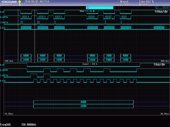
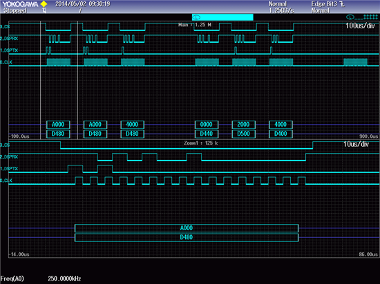
    Here's a couple screen shots. The first is with low voltages of nominally 0.1V on A0, A1 and A2. The second is with high voltages of nominally 2.5V on A0, A1 and A2. REFP is at 3V with respect to REFM.

    In both cases (screen shots) the ADC is first initialized with two writes of A000 followed by channel selects (conversion starts) of A2, A0, A1, A2.

    The following table lists the SPI tansactions shown in the two screen shots

    Trans:   1     2     3    4     5     6

    Low Voltage ~0.1V

    SDI:   A000  A000  4000  0000  2000  4000

    SDO:   2A90  2A90  2A90  2AA0  2AB0  2A80

    High Voltage ~2.5V

    SDI:   A000  A000  4000  0000  2000  4000

    SDO:   D480  D480  D480  D440  D500  D400

    In both cases, the responses (row SDO) in the last three transactions (columns 4, 5 & 6) are the conversion results for A2, A0 and A1.

    Low Voltage Case: The 5th response is 2AB where the LSB = 1 which is consistent with 12-bit resolution.

    High  Voltage Case: In all responses, the 2 LSB's (2^0 and 2^1) are 0. I didn't mention this previously but in addition to the LSB, the 2^1 bit also usually zero at the higher voltages. As voltage is increased, first the 2^0 bit sticks at zero then as voltage increases further the 2^1 bit also sticks at zero.

    I have inspected many conversion results, not just the first few shown here. The LSB's sticking at 0 at higher voltages is happening consistently. I have tested 3 different boards (chips).

    I have tried clock frequencies of 635 kHz and 250 kHz. The conversion results are the same.

    Karl

  • Karl,

    The interface timing does look clean.

    In the screenshots, you have zoomed into the A000 write access, rather than the data read access. Is it reasonable to assume that the number of clocks and other timing parameters are similar in these transactions as well?

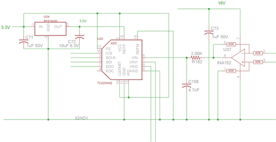
    Could you share the schematics of the circuitry around the ADC - supplies, reference and the input drive circuitry?

    Thanks.

    Regards,

    Sandeep

  • Here's a screen shot with a zoom into a read access. The voltage is nominally 2.5V. Notice there is some activity on the SPI where the ADC CS is not low. This is because the SPI is shared with a couple DAC chips.

    Here's the relevant portion of the schematic. The circuitry driving A0, A1 and A2 are the same. Only one is shown.

  • Karl,

    Thanks for the data. I am still trying to figure out what this issue might be, so I have a few more questions for you.

    You mentioned multiple devices on the SPI bus. Do we have an estimate of the capacitive load driven by the ADC on SDO? This can impact on the delay to SDO valid (tSCLK-DOV in the datasheet). But this is less likely to be the source of the problem, since you have tested at much lower speeds.

    Is there are buffer between the ADC and the DSP? If yes, on which side of the buffer are the SCLK and SDO probed?

    Looking at the table of transactions in your earlier mail, the absolute numbers for the low voltage case are actually worse than the high voltage case.

    - 0.1V should give a code of 0.1/3*4096=0x088 and the 0x2AB code you are getting would correspond to a ~0.5V input.

    - 2.5V should generate code 0xD55, which is close to what you have got.

    This does show up like a gain error in your system. What is the nature of the signal at the input of the amplifier? What kind of sensor/stimulus is it connected to?

    Could we try feeding a few DC voltages (say 0.5V, 1V, 2V, 2.5V) and noting down the ADC codes to figure out the transfer function we are seeing? It would help to observe the voltages at REFP and VIN pins of the ADC on a oscilloscope when doing the measurements to look for spikes.

    Regards,

    Sandeep

  • Sandeep,

    In the table of transactions I mistakenly listed ~0.1V for the low voltage case. It was ~0.5V.

    I need to set this question aside for ~1 mo. while I adress some more pressing issues. Please leave this thread open for now.

    Thanks,

    Karl

  • Sandeep,

    My coworker traced the problem to poor voltage regulation on the REFP pin. He fixed that and the ADC is now providing full 12 bit resolution.

    Karl

  • Karl,

    I am glad to hear that you were able to address the problem you were facing.

    I did suspect reference, which is why I requested that you monitor the REFP during conversions, but your schematic looks correct. You probably have an issue with the layout - placement or the routing between the reference IC and the ADC. Just to satisfy my curiosity, could you please let me know if you have the root cause for the poor regulation? Thanks.

    Good luck with your design.

    Regards,

    Sandeep

  • The voltage reference supplying REFP requires 10uF on its output but it had 0.1uF. Changing it to 10uF corrected the problem.