This thread has been locked.

If you have a related question, please click the "Ask a related question" button in the top right corner. The newly created question will be automatically linked to this question.

ADS7851 - Anti-Aliasing filter design for SDR

Other Parts Discussed in Thread: ADS7851, THS4521

Hi,
I am developing a SDR receiver as my bachelor thesis.
It is my first hardware project, so I got stuck on basics, probably.

Here is expected block scheme:

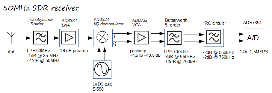
I will use a SDR concept, which contains an analog I/Q demodulator (AD8333) for mixing input frequency to lower.
Then will be signal sampled by A/D converter on 1,5 MSPS (ADS7851). So, Nyquist frequency is 750 kHz. But after mixing there are certainly a lot of strong higher frequencies.
I know, it is neccessary to use anti-aliasing filter. But what is sufficient value of attenuation on 750kHz?

I tried compute passive Butteworth filter 5. order - cutoff freq. 550kHz and attenuation on 750kHz is only -13dB. Because application is SDR receiver, it is important to reach cutoff frequency as high as possible for maximum bandwith.

There is a simple RC circuit described in ADS7851 datasheet:

I think, it will have not sufficient attenuation on 750kHz.

My theory:

Output signal range of VGA:   4V p-p
Voltage resolution of ADC:     (4 × VREF) / (2^N) = (4*2,5V) / 2^14 = 0,0006V
So, if there is an signal of frequency higher then 750kHz, with amplitude 4V (max), it should be attenuated below 0,0006V in ideal case.
10 * log(4/0,0006) = 38dB

Is it right?

Thank you!

  • Hello Filip,

    The ADS7851 is a SAR ADC, therefore the inputs of the device have to be driven with a low impedance source.  In order to obtain the expected performance,  the external driving circuit must be able to completely charge the ADC's internal sampling capacitor (40pF) to the target voltage within the allowed acquisition time.  In the case of the ADS7851, the sampling capacitor (Cs=40pF) must be completely charged and settled (within less than 1/2 LSB) within the acquisition period (90ns @ 1500kSPS) before the conversion period starts.  Since you are using the device at max data rate, you will require a differential amplifier to drive the ADC inputs.  The circuit on figure 45 (THS4521 and RC) is optimized to drive the ADC at max data rate providing low distortion results.  The R and C values are optimized for the driver circuit to be stable and settle within the acquisition time.

    This RC has a -3dB corner of ~9.7MHz which helps reduce the noise contribution of the THS4521; however, it does not provide enough attenuation for the aliasing signals present in this specific application.  Please note that if the RC time constant at the input of the ADC is too large, this will introduce distortion in the signal since the RC filter will not be able to settle in the required acquisition time. 

    Since there is a trade-off between settling/distortion and the anti-aliasing requirement in this case, my suggestion would be to perform the additional filtering stage prior the THS4521+RC that meets the needs of this application.  As you have mentioned, you will need to decide on the attenuation requirements based on the frequency and amplitude of the aliasing signals present in the application.

    Pages 23-27 provide good background into the ADS7851 input driving circuit needs.  In addition, please find below are a couple of application notes  examples that you may find helpful related to driving SAR ADC's.

    http://www.ti.com/tool/tipd117

    http://www.ti.com/tool/tipd115


    6607.forum_sampling_cap.pptx

    Thank you and Best Regards,

    Luis


  • Hello Luis,

    thank you for your explanation!