This thread has been locked.

If you have a related question, please click the "Ask a related question" button in the top right corner. The newly created question will be automatically linked to this question.

JESD204B with DAC37J82/ADS54j54

Other Parts Discussed in Thread: ADS5400, ADS54J54

I have used GUI for configuration setting so far.

I have both EVM board of DAC and ADC and the project that i have practiced on KC705 is "jesd204_hwdemo"


The first concern is that

I hope that there is another way to write registers with SPI directly, not using GUI setting.
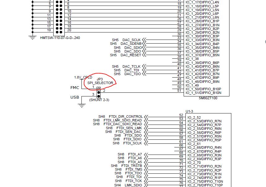
(I think EVM board has SPI on it)

Is there another way to use SPI for register setting fof DAC/ADC??

If so, is there any instruction about writing register value with SPI?
or Does any one can tell me about the process of using SPI on KC705?

The second concern is that

Do you think ther is a special/hidden register that I can adjust for the amplitude or
delay the input on ADC 54j54 ?

if so, can you tell me how to adjust?

Last question is that

After saving/loading the value, when i open the .cfg file,
I can see some special address / register value which is not on the datasheet.

Can you tell me about the purpose of these register?

I appreciate for any help or comment

Thank you

  • Hi, Inhwan;


    For the DAC case:

    On the EVM of DAC3xJ8x, we do not reserve SPI jumpers of DAC as I have checked. We use the GUI communicate with the EVM board through USB interface. FTDI chip FT2232 is used to convert USB to SPI. The SPI of FT2232 communicate with DAC's serial control interface through CPLD. Attached is CPLD code, and hope it can help.

    Sorry, I am not an FPGA guy, so not familiar with KC705.

    For the last question, can you give me the specific register information of .cfg file, then I can deal with that?

    Thanks a lot!

    Yarn.8688.DAC38J84_CPLD.rar

  • Hi,

    For the ADC54J54 I am not aware of any SPI registers to control the aperture delay or adjust the input gain.   On some other devices I have seen such adjustments possible by way of SPI register writes such as with the ADS5400, but not with this device.    There are some coarse adjustments of full scale input as shown in Table 33, and there is an option to use an external reference voltage shown in that table.   When an external VREF is used, it is often for the purpose of having a more fine control of the full scale range of the ADC than the internally generated reference voltage provides.   But I do not see a section in the datasheet on the usage of external reference.  If that is of use for your issue, then I can look into that further. 

    The datasheet for the ADS54j54 is in the process of being updated.  There are some internal trim registers that are accessable by SPI and that should always be written at power up or after reset for optimal results - and these trim registers are what you are seeing in the SPI cfg files. 

    The full list of initialization steps required for the ADS54J54 is as follows:

    7.3.13 Device and Register Initialization

    After power-up, the internal registers must be initialized to their default values through a hardware reset by

    applying a low pulse on the SRESETb pin (of width greater than 10 ns), as shown in Figure 1. If required later

    during operation, the serial interface registers can be cleared by applying:

    • Another hardware reset using the SRESETb pin

    • A software reset (bit D0 in register 0x00). This setting resets the internal registers to the default values and

    then self-resets the RESET bit (D0) back to 0. In this case, the RESET pin is kept high.

    • Write the following data to the registers after every device power-up or reset for optimum AC performance

    Address Data Reason

    0x06 0xFFDF Turn off fuse logic for power savings - not required

    0x44 0x0074 Trim value - required

    0x47 0x0074 Trim value - required

    0x4C 0x4000 Trim value - required

    0x50 0x0800 Trim value - required

    0x51 0x0074 Trim value - required

    0x54 0x0074 Trim value - required

    0x59 0x4000 Trim value - required

    0x5D 0x0800 Trim value - required

    Regards,

    Richard P.

  • Hi Yarn Guo

    First of all, thank you for reply.

    However, I am just wondering the purpose of SPI_SELECTOR on the DAC schematic

    I thought I can use SPI directly for register setting because schematic mentions about SPI_selector.

    The answer for the specific register information of .cfg file is given below by Richard.

    Anyway thank you for help

  • Thank you for help.
    I got confused between DAC and ADC. I just checked out the existence of SPI on schematic. However, it wasn't on the schematic.
    Anyways, Thank you for the specific registers information.
    For Vref information, let me try it first and I will ask you about further information that i need.
    Thank you
  • Hi, Inhwan;

    The SPI selector is used to select whether the SPI host comes from FPGA through FMSC or from GUI through USB.
    Thanks a lot!

    Yarn.