This thread has been locked.

If you have a related question, please click the "Ask a related question" button in the top right corner. The newly created question will be automatically linked to this question.

ADS54J54EVM FMC Connection

Other Parts Discussed in Thread: ADS54J54EVM, ADS54J54, LMK04828

Hello,

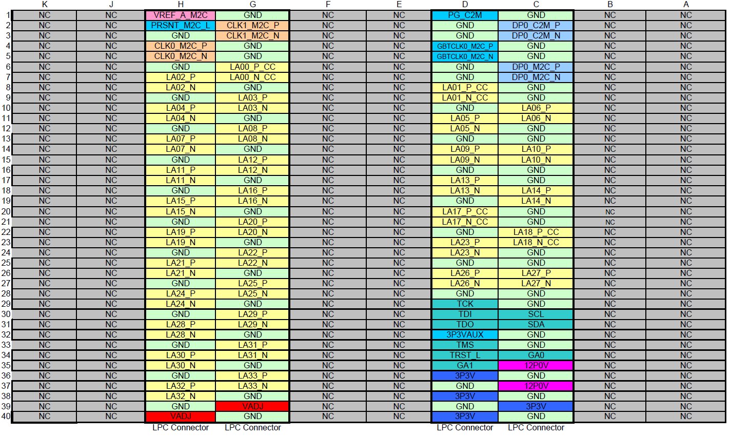
With regards to the ADS54J54EVM ADC Evaluation Module, I've noticed that on the provided design package on the schematic file, the FMC pins seem not to be wired according to the LPC configuration (currently our development is on the Avnet Kintex-7 Mini-Module Plus board, with banks CDGH wired into the FPGA as per LPC).  

Is the schematic accurate, and if so, are there ways (i.e. boards, connectors) that can adapt the current ADS54J54EVM FMC pin configuration into ones that comply with LPC?  

Thank you.

  • Hi,

    the schematic is accurate, so the 8 lanes from the ADC are routed to the FMC connector as shown in the schematic.  In our TSW14J56 we have the FPGA (Altera) firmware simply capture the 8 lanes of data into memory and after uploading to the PC we sort out which bits go with which channel.   So we can remap lanes.    But we also have firmware to let the EVM work with either a Virtex or Kintex development platform, and for the Xilinx firmware there was also the ability to remap lane assignments into the Xilinx JESD204b IP, but in that case we did not create that firmware - someone from Xilinx created that firmware for their platform.   For the Virtex development platform we have the 8 lanes of data from our ADC routed to the lower 8 lanes of the JESD204b link through the FMC connector so we can still get all 8 lanes of data.  But I believe the Kintex development platform only had four lanes of JESD204b data through the FMC connector to the FPGA, and even with our ADS54J54 in 4-lane mode only two of the ADC channels are on lanes that the Kintex development platform would support.    We do not have an adapter built to physically remap any of the JESD204b lane assignments.

    Regards,

    Richard P.

  • Hi Richard,

    Thank you for your reply. I just wanted to clarify a little based on the information you've given me:

    The 8 Lanes refers to the differential pairs of DA ... DD [1:0] coming from the ADC into the FMC pins if I'm not mistaken.
    With regards to the Virtex configuration, that would be all 8 differential pairs going into the FPGA from the 4 ADCS (if I'm not mistaken).

    You mentioned that the ADC can be set in 4 lane mode : I'm assuming that since you mentioned that even activating this mode only two of the ADC channels would be available, 4 lane mode simply reduces the data width. I'm also assuming that the reconfiguration of the lanes only changes which pins/banks they sample (please correct me if I'm wrong).

    However, our current board uses a XC7K325T - 1FFG676 FPGA, with one FMC LPC connection available, which, through an inspection of both the Avnet schematic and your (TI) schematic, only connect to 1 differential pair/lane of data (as they only coincide on the C, D, H, and G rows), unless the firmware can somehow modify the physical wirings as well (which I doubt).

    Do you have any suggestions as to how we can interface these two components without sacrificing 7 lanes of data ?
  • Hi,

    You're losing me there.  I don't know the pinout of the FMC connector on the board that you are using.  Could you post a screenshot of that portion of the schematic please?  I see our 8 pairs being on sections A, B, C of the FMC connector, with 5 of the pairs being in segment A, two more in segment B, and another in segment C.  And this is the same pin assignment for these 8 pairs that are used by both the Altera and the Xilinx development boards that I am familiar with.   We don't have any JESD204b lanes on rows D, H, G.    Where we have run into issues is that we don't always start with lane 0 in our lane assignment.   The 'standard' lane assignment shared between Altera and Xilinx for this connector has specific pins called out for lane0, lane1, lane2, etc.   And if you put the ADS54J54 into 4 lane mode you do not see only lanes 0 through 3 in use.  Rather it is lanes 1,2,5,4.   The Kintex development platform that we have in hand here only connects lanes 0 through 3, meaning we cannot get data from the ADC to the FPGA for channels C and D at all.   If your lane assignment to your board's FMC connector is different, then we cannot do anything to fix that.

    Ah, I think I see the issue.  You did say LPC, and that is a different thing.  Are you looking at the pin assignment as in the attached table?  Those diff pairs generally go to FPGA pairs that are capable of supporting LVDS inputs or outputs, or single ended IO, but not 8b/10b coded high speed serial lanes that would go to the SERDES lanes of the FPGA.   For example, most of our EVMs that have LVDS IO use a connector from Samtec, and we have an adapter board that maps the EVM Samtec connector to the FMC LPC pinout to get the LVDS up to the LVDS capable input pins of the FPGA.    The FMC pin assignments for the JESD204b lanes are completely different.  Not the LPC pin assignment at all.   I am not aware of any development platform that routes the LPC dif pairs up to the FPGA SERDES IO.  Just FPGA LVDS IO.

    Regards,

    Richard P.

  • I see, that makes things so much clearer, thank you, I had not realized only GTX RX differential lines could be used for the JESD specification!

    With the pins configured as they are, I believe our board's LPC FMA only connects to the DP0 GTX rx line on the board (as per the diagram you posted), and DA1 on the EVM (Which I assume is Lane 1).
    Assuming that we configure the board into 4 channel mode, would it be possible to run that one lane configuration with the pins exposed by the LPC standard? (i.e. no OVRA-D signals and no SYNC signal on row K (which I believe goes into the clock module)?
  • Hi,

    No, I don't see a way to use the LPC pinout at all.   The only data pair from the ADC that makes its way to the FPGA is the DA1 pair, as noted.   If the ADC is operated in 8-lane mode then this one pair only carries half of the data from channel A as shown in Table3 of the datasheet.  And if the ADC is operated in 4-lane mode, then the data from channelA is on pair DA0 as shown in that same table, and no data is on DA1 at all.     Plus in order to complete a JESD204b link there are other signals that need to connect from the EVM to the FPGA through the FMC connector, namely the device clock from the LMK04828 on the EVM to the JESD204b IP that would reside in the FPGA firmware, the SYSREF from the LMK04828 to the FPGA, and the SYNC signal from the FPGA back to the ADC.  All these signals are on defined locations on the FMC connector pinout that is used for the JESD204b link.

    Regards,

    Richard P. 

  • Hello,

    I see, I originally thought that since you said that 4 lane operations were on 1 2 5 4, that DA1, as well as the other signals wired on the C D G H banks (i.e gtx_clk, clk_la, car_sysref, syncab, synccd) would be accessible, and that we could hook up the LMK04828 clock sync signal externally, ditching the OVRB signals and the clk-p clk-m and sys_p sys_m signals (which the KC705 also has as NC according to their schematic).

    But if 4 lane operation doesn't output to the LPC lane DA1, and there is no way on the EVM to modify which pins each lanes output to, then there's not much that can be done.

    Thank you for your time and help Richard!

    David