This thread has been locked.

If you have a related question, please click the "Ask a related question" button in the top right corner. The newly created question will be automatically linked to this question.

ADS8860: Layout for multiple channel ADC conversion with single voltage reference

Other Parts Discussed in Thread: OPA376, OPA625, ADS9110EVM-PDK, ADS8860, ADS8881

Hello,

Regarding the composite buffer you proposed here, could you please take a look at the layout for the composite buffer (OPA378+OPA625) and the connection of the 4.5V reference voltage to the ADS8860.

I'm using a 4-Layer PCB (Signal/GND/Power/Signal). For space reasons I was not able to put the output of the composite buffer closer to the reference input-pin of all the ADS8860. I used for this a polygon on the bottom layer and then I connect this signal to the top layer using vias (0.3mm/0.6mm) to another polygon connected to a resistor (R14 / 0.22Ohms) in series with the local capacitor (C23 / 10uF). 

I would appreciate your thoughts on this.

Thank you and kind regards,

Sebastian

  • Hi Sebastian,

    The layout looks clean in general.  A couple of suggestions:

    On Reference Driver Circuit: 

    -U4 (OPA376) appears to be missing V+ supply bypass Capacitor.  Please use a 0.1uF X7R capacitor.

    - U5 (OPA625) appears to be missing V+ supply bypass capacitor.  Please use a 10uF X7R 10V capacitor.

    Just for reference, below is the ADS9110EVM-PDK userguide; showing a similar reference driver schematic/layout circuit.

    www.ti.com/.../sbau249.pdf

    On ADC Layout:

    - The SAR ADC inputs require an RC filter to reduce the input  amplifier driver broadband noise and to attenuate the effects of charge kickback or charge injection.  The filter capacitor needs to be in very close proximity to the ADC inputs, AINP and AINN. 

    -  Best practice is to place the AVDD bypass capacitor on the top layer, avoiding vias between the AVDD pin and the AVDD bypass capacitor, since vias add some inductance in the path; If possible, please change the AVDD bypass to top layer.

     If is not possible at all to place the AVDD bypass capacitor on TOP layer due to space constraints, use an isolated via to directly connect the AVDD pin to the AVDD bypass capacitor on bottom (i.e., ensure this via is not connected to the AVDD power plane and this via is only connected to the AVDD bypass capacitor and AVDD pin); then use a second separate short trace/via on bottom to connect the AVDD bypass capacitor to the AVDD plane. This will ensure the AVDD pin sees effectively the bypass capacitor prior the power plane.

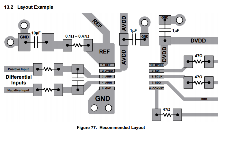
    The ADS8881 datasheet, which is a device from the same family (ADS8881 18-B version with differential input) offers a layout example on Figure 77 (p.47) and a section on board layout recommendations.  The only change will be on this case, the RC filter is single-ended for ADS8860.


    If you have the schematic of the circuit used to drive the ADC, we could review as well.

    Let me know if you have questions.

    Thanks and Regards,

    Luis