This thread has been locked.

If you have a related question, please click the "Ask a related question" button in the top right corner. The newly created question will be automatically linked to this question.

How to synchronize multiple ADCs and FPGAs across JESD204B link

Other Parts Discussed in Thread: ADC12J4000, LMK04828

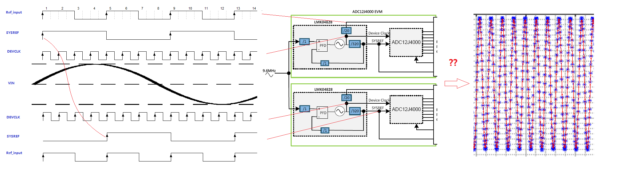
I recently learned how to use the Jesd204 ADCs,there is a example design Synchronizing Multiple ADC12J4000 ADCs 'tidu851'.

I have some questions about Jesd204B-1 clock configuration:

1.about LMK04828:

'SYSREF_A' and 'DEVCLK_A' on each ADC12J4000 EVM should be phase aligned,so  a common SYNC must be posted to each LMK04828 'SYNC/SYSREF_REQ' input  on each ADC12J400 EVM? but i see no such wire connection.

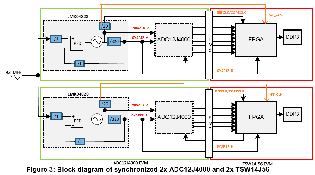
2.about FPGA device clock:

FPGA Jesd204B RX need a 'refclk' and 'glbclk' which corresponding to 'GTX reference clock' and 'core clock',does  'refclk' and 'glbclk' must all be phase aligned(core clock is needed when core clock is greater than 165MHz or not equal to reference clock)?

  • Hi min hu
    I'm reviewing the questions and will respond later today.
    Best regards,
    Jim B
  •  i am learning how to use Jesd204 device , plan to design a 12 channel synchronous sampling system,made up of three boards,4 channel each.

    Sampling rate = 480Msps, FPGA refclk = 120MHz, SYSREF = 7.5MHz

    The reference input of the three boards is provided by the splitter with common 20MHz

    I plan to use LMK04828,it is a complicate device,synchronization of multiple LMK04828 is critical. 

  • Hi min hu

    1) The architecture used in that diagram does need the internal LMK04828 dividers to be initialized. The use of 0-delay feedback mode from the SYSREF output to the reference input ensures the SYSREF output of each LMK04828 will be phase aligned to the input reference (at F_SYSREF). To ensure the clocks for the FPGA are also aligned, the internal dividers must be reset/initialized. That can be done using either register writes alone or a combination of register writes and logic signal inputs to the SYNC input pin.

    2) To ensure consistent alignment of the 2 ADC+FPGA systems, the FPGA clocks should be phase aligned with SYSREF.

    The presentation at the link below describes the methods to initialize the LMK0482x dividers, and then configure the device for the desired SYSREF output mode.

    https://e2e.ti.com/support/clocks/m/videos__files/666599


    I hope this is helpful.

    Best regards,

    Jim B

  • Hi Jim B

    thanks for your reply
    ---------------------------------------------------------------------------------------------------------------------------------------------------------------------
    1) The architecture used in that diagram does need the internal LMK04828 dividers to be initialized. The use of 0-delay feedback mode from the SYSREF output to the reference input ensures the SYSREF output of each LMK04828 will be phase aligned to the input reference (at F_SYSREF). To ensure the clocks for the FPGA are also aligned, the internal dividers must be reset/initialized. That can be done using either register writes alone or a combination of register writes and logic signal inputs to the SYNC input pin.
    ---------------------------------------------------------------------------------------------------------------------------------------------------------------------
    SYSREF output of each LMK04828 is phase aligned to the input reference,--->DCLK output is phase aligned to the SYSREF,
    --->since SYSREF is the lowest frequency,DCLK frequency is inter multiple of SYSREF,DCLK of multiple LMK04828 is phase aligned even each LMK04828 internal dividers are reset at difference instant.
    the key is :DCLKs frequency must be 2^n integer multiple of SYSREF,right?

    in the figure above,DCLK2 is phase aligned with SYSREF,DCLK3 is phase aligned with SYSREF,but DCLK2 and DCLK3 are not phase aligned.using register writes can not sync two LMK chips,even in 0-delay mode.


    ---------------------------------------------------------------------------------------------------------------------------------------------------------------------
    2) To ensure consistent alignment of the 2 ADC+FPGA systems, the FPGA clocks should be phase aligned with SYSREF.
    --------------------------------------------------------------------------------------------------------------------------------------------------------------------
    both the refclk and coreclk(external) should be phase aligned with SYSREF?

  • Hi min hu

    1) As long as the DCLK frequencies are an integer multiple of the SYSREF frequency it will be possible to get consistent SYSREF capture by the FPGA. If they are integer frequency multiples there will be a rising edge of DCLK aligned with every rising edge of SYSREF. Of course depending on the VCO frequency and SYSREF frequency, not all integer multiples of SYSREF can be created from the high frequency VCO frequency.

    2) I think it is best to phase align both FPGA clocks, but I believe the coreclk is the most critical one for the Xilinx JESD204B IP. That is the one used to capture SYSREF. The refclk is used for the serializer PLLs so the phase shouldn't matter as much. If only a single clock is used to provide both the refclk and coreclk, then it must be phase aligned with SYSREF

    Best regards,

    Jim B

  • thanks for your reply

    device clock for ADC/DAC and reference clock for FPGA RX are phase aligned with SYSREF in each EVM-board,The deviceclock and reference clock of the two boards are aligned with each other,but SYSREF are not aligned with each other.

    The sampling instant is the rising edge of the sampling clock,so i should get the same sampling data;

    clocks are sync with SYSREF,so the link latency should  be the same;(each individual board looks exactly the same!)

     reference clock for FPGA are phase aligned,so sampling data can be buffered and captured by the same clock edge.I should see perfectly identical sample tracks, is it right?

    SYSREF phase relationship between multi-boards seems to be irrelevant?

  • Hi min hu

    The High Speed Data Converter Pro firmware and software capture a block of data with the start point aligned to the start of the FPGA local multi-frame (LMFC) boundary.

    The FPGA LMFC is aligned to the SYSREF applied to the FPGA and the ADC LMFC is aligned to the SYSREF applied to the ADC.

    If there is a misalignment between the SYSREF on the two boards, the captured data blocks in the two systems will be offset in time due to the LMFC misalignment. If the same waveform is input to both ADC12J4000 boards, the waveforms will be offset when the two data blocks are compared.

    To keep the waveforms aligned in the data, the SYSREF of the two systems must be aligned to each-other. This is done by applying the input clock at F_SYSREF, and using the 0-delay feedback feature of the LMK04828 devices to align the output SYSREF to this input reference.

    Best regards,

    Jim B

  • Hi , Jim B
    the data streem are sync,if a capture data by DIVLK edge instead of SYSREF(SYSREFs are not aligned),there will be no offset,right?
  • Hi min hu

    The JESD204B IP from FPGA vendors all use the LMFC frame boundaries to align the captured data output from the de-serializer blocks and sent to the downstream logic.

    Even if you wrote your own capture IP from scratch some of the data formats will not allow you to generalize the data capture to octet or sample boundaries. Some formats have added Tail bits at the end of each frame, or every second octet, etc.

    See Tables 12 and 13 of the ADC12J4000 datasheet for examples.

    So sometimes the data must be handled on a frame boundary perspective at minimum.

    Best regards,

    Jim B