This thread has been locked.

If you have a related question, please click the "Ask a related question" button in the top right corner. The newly created question will be automatically linked to this question.

ADS1130: ADS1130 is giving me half the expected result

Part Number: ADS1130
Other Parts Discussed in Thread: ADS1230

Hi,

I am a hardware engineer in Weighing machine Industry. I am making one low cost 40Kg machine having 2gm accuracy based on TI ADS1130 part. In my design ADS1130 is been interfaced with 8 bit micro controller which is serially connected with ADS1130 part.  Load cell specification is as below:

LOAD CELL SEPCIFICATION

Rated Capacity

40

Kg

Excitation Voltage

5

V

Rated Output

1.955

mV/V


I am giving 5V to AVCC & 3.3V to DVCC.

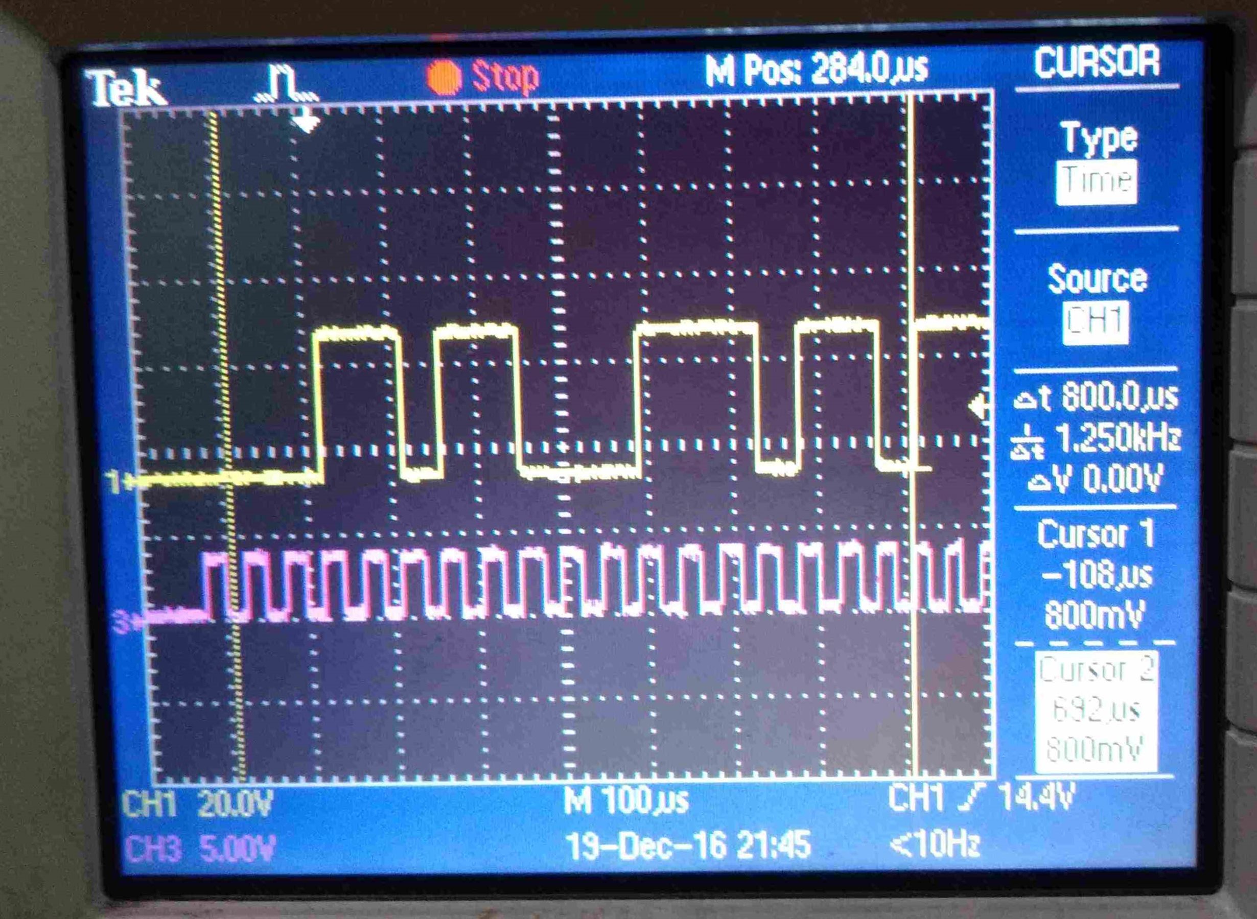
According to above data, at Full load capacity of Load cell, I will get max voltage of 9.775V & ADC Count I should get 65599. But I am getting exactly half of it i.e. 32799. At any weight, corresponding output in ADC count I am getting half of what is theoretically expected. I have verified my schematic, component values and board voltages. All are perfect. Then I verified the data output from ADS1130 on CRO & found also that output data is coming exactly half which shows there is no bug at software side, the data itself is coming half to what is expected.

In order to verify my mistake, I checked one of my competitor product that is using the same ADS1130, there I observed a mysterious thing that he has connected DVCC to pin no 4. Pin no 4 in ADS1130 is actually DGND even than he has connected it to DVCC. I did same thing on my board & immediately I started getting correct result. At full load now I am also getting 65599, but it is beyond my imagination how it is working? How an ADS1130 IC started giving me correct result on applying DVCC at 4 pin which is meant for GND. How this pin is correcting its GAIN? I checked there are no errata on this product. Technically can you guide me on this behaviour of ADS1130 part?  

Here I am attaching my schematic & the snap shot of CRO showing the data+Clock signal at 32kg weight.3010.ckt.pdf
  • Hi Krishan,

    You have miscalculated full-scale range of the ADS1130 which is +/- (1/2) Vref/64. When connecting pin 4 to DVDD you are changing the operational parameters of the ADS1130 which is outside the device specifications and tested mode of operation.  If you want higher gain and performance you should use the ADS1230.

    Best regards,

    Bob B

  • Dear Krishan,

    as Bob mentioned, the confusion is most likely coming from your calculations.
    The ADS1130 offers a PGA Gain=64 and the input voltage range of the ADS1130 is specified as VIN = +/-0.5*VREF/64.
    The LSB size of the ADC is 2*(0.5*VREF/64) / 2^18 = (5V/64) / 2^18 = 298nV.
    That means at full capacity you will read a code of (5V*1.955mV/V) / 298nV = 32802 which is almost exactly what you are seeing.
    That means the results your are getting are absolutely correct.

    Your competitor seems to be operating the ADS1130 in an officially unsupported and untested mode.

    Regards,

  • Hi Bob,

    Thanks for your prompt clarification.

    Further to it, I want more support on my problem :

    1. Is there a way to calibrate ADC input offset itself @ no load? Like we have in ADC1230 by giving 25 pulses as mentioned in the datasheet. What is the similar recommended method for ADS1130 for this No load offset calibration ? 

    2. I am using 40Kg load cell running with excitation voltage of 5V & having a rated output of 1.955mV/V & target is to achieve 2gm accuracy. Can I achieve it with ADS1130 practically? 

    3. You must have seen my schmatic in previous query. Do I need some improvement it in terms of component value/ positioning apart from layout.

        I have added 100E resistance at REFP & REFN pins & same as on AINP & AINN. Is it correct to achieve good differential result? 

    At present I am hunting to achieve this 2gm accuracy & could not able to achieve it.  

    regards,

    Krishan

  • Hi Krishan,

    Regarding 1, although the ADS1130 is similar to the ADS1230 certain features are not available for the ADS1130, like the internal offset calibration.  For your application this is not required as there is also sensor offset error of the bridge that must also be removed.  The best thing for you to do is a 2 point calibration where the no load condition of the bridge is 0 weight.  The returned code with 0 weight is subtracted from any further result.  The second point for calibration should be with a known calibrated weight applied that is near the value of the full-scale capacity of the load cell.  The slope of the no load and known load gives you the grams/code of the measurement.

    Regarding 2, you should be able to achieve 2 gram resolution for 40kg load cell at 10sps.  Your best case resolution will be with shorted inputs.  If you have layout or supply noise issues this will show up as a noisy result. You should be able to see no more than 1 code (bit) of noise in the shorted input case.  When attaching the sensor to your PCB, there may be additional noise sources such as power line cycle noise, or EMI/RFI.  This external noise will directly impact your measurement and will need to be prevented from entering your ADC input.

    For 3, you generally have a good starting point, but due to any external noise sources that may enter your system you may need to add additional filtering components.  What components you add will depend on the sources of noise you encounter.  Also, as the measurement is ratiometric where noise/drift of the excitation source should cancel in the measurement, there is an assumption that the noise and filtering is the same for both the reference input and the analog input.  This is often difficult to achieve without using a 6-wire load cell where the reference input is a Kelvin connection from the sensor.  Also note that the reference RC filtering differs in your circuit with respect to the analog input filtering (primarily the differential caps).

    Best regards,

    Bob B

  • Hi Bob,

    Happy New Year.

    I am still getting weighing error of 2gm.

    Machine Full Scale

    0kg to 40kg

    Calibration method:

    Two point - At zero load & at 2kg (Customer doesn't want to do calibration on higher weights)

    Issue Description

    With this configuration, if generally have 1 bit error at 2 points (no load & running load [0 to 40 kg])

    These 2 errors gets added up & make a error of 2 ADC counts (equal to 1.6 gm in my case).

    This lead to breach my requirement of 2 gm minimum resolution as the SW algorithm shows it as 1.002kg for 1kg load, due to SW rounding.

    Algorithm used:

    I used SINC4, with moving average with 16 samples as the window size. Final result is rounded to the near multiple of 2gms.

    Please suggest how can I achieve dead stable output on standard loads.

    2nd problem, linearity is also a big issue, not getting linear graph of my display value for a constant calibration slope.

    Please suggest on these two problems.

  • Hi Krishan,

    I'm not surprised that you are seeing a linearity error when you are calculating the gain slope with only 5% of the full-scale capacity of the load cell.  This small of a voltage output for the load cell will not account for any non-linearity of the load cell itself, nor will it account for any gain error of the ADC.  Also remember that even with full-capacity applied to the load cell it is only about 1/8 of the full-scale range of the ADC.  So 2kg is too small to determine the gain slope.

    Another thing is you cannot really tolerate any additional system noise.  Averaging may not help.  Without averaging you should see return values that fluctuate by no more than one code.  You are seeing this with averaging, so I suspect that your system is noisy.

    Best regards,

    Bob B

  • Hi Bob,

    Major issue with the product right now is Repeat-ability, linearity errors I will handle differently.

    Same load kept again & again on the system, sometimes, shows error of 2-4 gms (for 40kg full-scale).

    I tried new layout of the PCB too, situations improved, but still some times +/- 2 to 4 gms error gets displayed.

    I am worried, that my 1 code is equal to ~0.8 gms, so this is accounting to a error for 3-4 ADC counts. 

    Please suggest that is the main issue in getting repeat-ability on standard weights measurement.

    * I am measuring 1) No load reading 2) Running weight reading.

    * No load is taken in account after sufficient stabilization of load cell output.

    * All measurement is done thru SINC4 filter with moving average algorithm.

    Thanks,

    Krishan

  • Hi Krishan,

    As I mentioned early on in this thread, sources of external noise are of great concern.  If you are using averaging and are seeing this much deviation, than you have a lot of noise outside of the ADC.  You will need to determine the source of the noise and then properly eliminate it with filtering components and/or shielding.  Most noise I've seen entering the ADC input circuit is due to noise pickup on the cable from the load cell to the PCB.

    Best regards,

    Bob B