This thread has been locked.

If you have a related question, please click the "Ask a related question" button in the top right corner. The newly created question will be automatically linked to this question.

ADS8860EVM-PDK: ADS8860 - Not understanding readings coming out of device

Part Number: ADS8860EVM-PDK
Other Parts Discussed in Thread: ADS8860

I'm using an ADS8860EVM-PDK, but I've detached the board containing the ADC itself and connected it to a C2000 device.  I'm running the CONVST signal with a PWM (1us on, 100kHz freq), and running a 20MHz SPI clock.  It is powered by a 5V supply and I've connected all essential signals according to the ADS8860EVM-PDK User's Guide (SBAU213).

I'm using a function generator to provide a DC signal and am attempting to map the DC voltages to the values read by the C2000 out of the ADC.  JP4 jumper is open, which should be 0-4.5V on the input of the circuit means 0-4.5V on the input to the ADC (inverted).

When I sweep across the range, I get this:

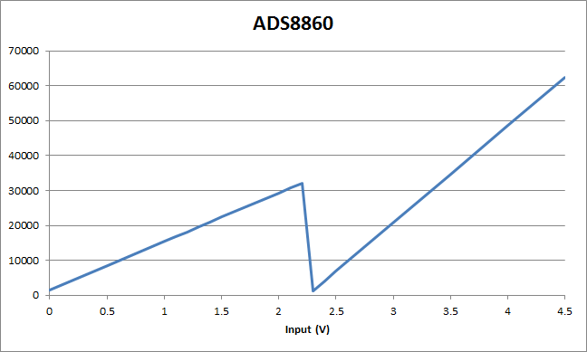
The fact that it restarts at exactly half the range (as well as the slope difference being 2) indicates it's something simple like I'm just interpreting the bits wrong, but can't figure out how according to either of the documents (EVM User Guide or the ADC data sheet).

Should the 16 bits be signed or unsigned?  

Are there any shifts or scaling necessary out of the raw SPI buffer?

Is it possible I'm reading the bits out in the wrong order?

Thanks!

  • Hello James,

    The ADS8860 is a single-ended device, data format is straight binary, unsigned. No scaling is required, the output is a function of VREF (1LSB is equal to VREF/2^16). The device interface supports different modes of operation , 3-  or 4-wire interface, using the busy indicator or without.  As you have mentioned, the ADS8860EVM-PDK has an an amplifier on the inverting configuration, supporting unipolar 0-4.5V input when JP4 is open. 

    For example, below is figure 49 from the datasheet showing the 3-wire CS mode without BUSY indicator (DIN=1).  In this case CONVST functions as CS and should be brought after the max conversion time lapses (710ns).  Notice, the MSB (D15) is updated immediately when CONVST is brought low; and updates to (D14) on the following falling edge of SCLK.  Is it possible you are not capturing the MSB?

    You have mentioned that you are operating the device at 100kSPS, (1uS on, 100kHZ PWM) with 20MHz SPI clock: 

    -          Which serial mode of operation is being used (i.e. 3-wire/4-wire mode w Busy or without BUSY)?    Can you please provide a diagram of the EVM digital interface connections, supplies and the analog side function generator connections?

    -          Are you reading DOUT on the falling edge or rising SCLK edge?   Please provide an oscilloscope plot of the data read frame, showing the interface signals:  CONVST, SCLK, DOUT and DIN (please place the oscilloscope probes in close proximity to the ADC pins) while applying a  +1.0 V DC signal at the input of the inverting amplifier (should yield +3.5V at the ADC input):

    Thank you and Best Regards,

    Luis

  • Hi Luis!  Thanks for the reply.

    I'm using the 3-wire mode w/out Busy.  I'd provide a diagram, but your second bullet point was the piece I was missing.

    I had modified the clock polarity and phase out of my C2000 master device and I am getting correct readings now.

    This part of the document:

    "Data are valid on both SCLK edges. Data are valid on both edges of SCLK and can be captured on either edge."

    made it seem like that didn't matter.

    Thanks again!

  • Hi James,

    That's great news, many thanks for letting us know it is working.

    In order to read SDO on the falling edge, the controller has to be able to read SDO within th-CK_DO, which is a tight timing spec, and requires a fast controller. 

    I agree with you, on most controllers, the user will read SDO on the rising edge.

    Let us know if you require anything else.

    Many Thanks,

    Luis