This thread has been locked.

If you have a related question, please click the "Ask a related question" button in the top right corner. The newly created question will be automatically linked to this question.

ADS1256: Sample code for ADS1256?

Part Number: ADS1256

Hello,

I have a DK-TM4C129X dev kit that I would like to interface via SPI to the ads1256evm-pdk performance kit.  The performance kit has ADC Pro that can be used to sample the channels; however, it appears as though you can only look at a single channel at once.  I'd like to look at three channels at once, so I was considering writing a SPI interface to the DK-TM4C129X dev kit to display the samples to the LCD and/or log the samples to the SD Card.

The code itself doesn't necessarily need to be TIVA 129 specific (that'd be great if it was).  I'm just looking for sample code that puts the SPI bytes together that properly configures the ADS1256 to help speed up our development.

Thanks!

  • Hi Aaron,

    There are a several examples projects for the ADS1256 scatted around E2E. Here are links to the example projects that I'm aware of:


    Multiplexing the ADS1256 with the MSP430 (I created this project so I'm familiar with this code):


    Another ADS1256 and MSP430 project can be found here:

    ftp://ftp.ti.com/pub/data_acquisition/ADS1256_on_HPA449/ads1256evm_dist.zip


    Example code using the C641x

    There is also a third-party project on GitHub with example code for an Arduino, found here:


    I hope that helps!

    Best Regards,
    Chris

  • Hi Chris,

    The MSP430 example code you wrote looks helpful and promising.

    Quick question, for your "busywait" routines. When specifying delay of 35/150, is there a specific period of time you were hoping to wait for on these delays (I'll be running a faster processor and wish to understand better the delay times you were trying to achieve).

    #define DELAY_RDATA() busywait(35) //Delay
    #define DELAY_RREG() busywait(150) //Delay

    Thanks,
    Aaron
  • Hi Aaron,

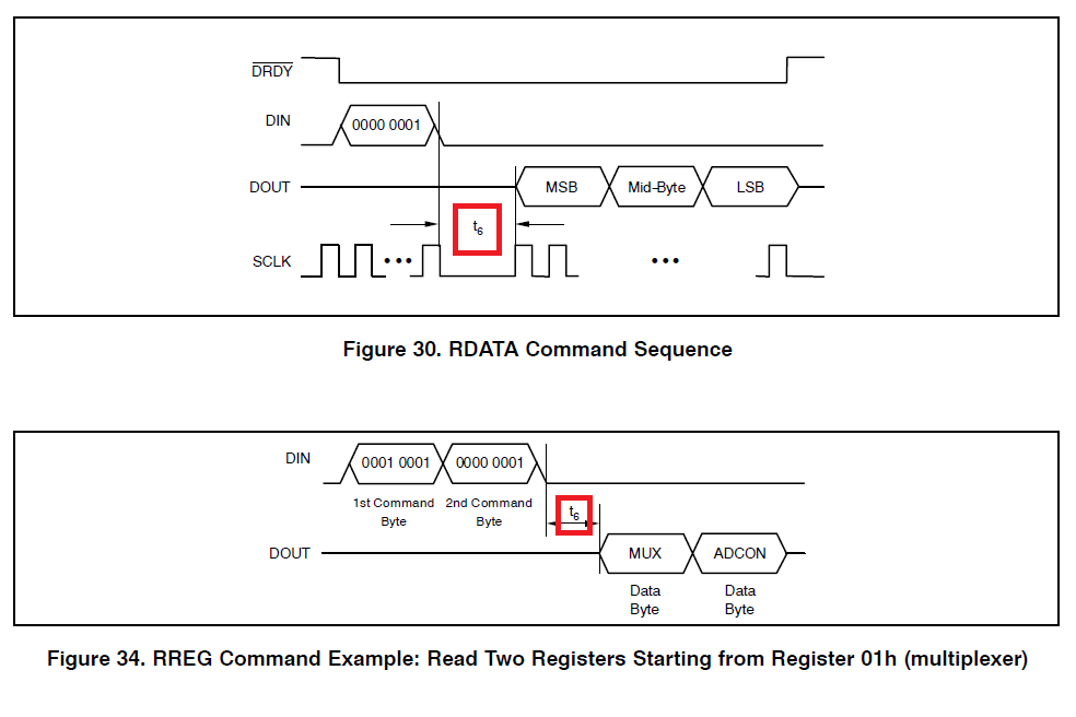
    I believe I got those specific delays out of another project, but in effect all they need to do is provide for the ADS1256's t6 timing specification. Both RDATA and RREG need a short delay between the command and data bytes as shown below:

    It also looks like I commented out the only place where "DELAY_RDATA()" was called in the code. I believe with the MSP430's 8-bit SPI transfers, there was a built-in delay when waiting for the single byte SPI transfer to complete. So in my case it really wasn't necessary to provide these extra delays at all, but it's still a good idea to keep a placeholder or reminder that a delay would be required on a faster processor.

    Best Regards,
    Chris

  • Hi Chris,

    Thanks for the explanation.

    I have a follow-up question on the code.  It appears as though you're waiting for 3 pulses on the DRDY line before acquiring the sample.  I'm curious if there is a need for this?  

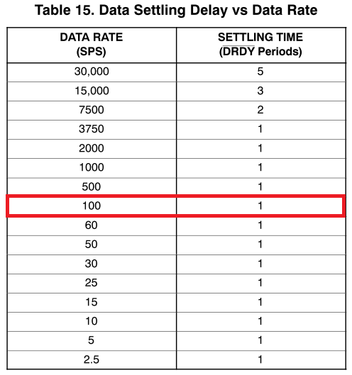
    I was looking through the datasheet on page 22 table 15 and it seems for 100 SPS, that you should be able to use the reading on the first falling edge of DRDY (you wouldn't need to wait 3 unless your SPS was set to 15,000).  Am I interpreting this correctly?

  • Hi Aaron,

    I believe that the 3 /DRDY pulse delay is unnecessary and that you're understanding is correct!


    If you restart the ADC conversions (by sending SYNC and WAKEUP), then you shouldn't need to wait for multiple /DRDY pulses...data will be settled on the next /DRDY pulse (though for the faster data rates you'll notice that the first /DRDY pulse is delayed to allow for this settling).

    (NOTE: Keep in mind that your input signal must already be settled when start an ADC conversion. For example, if an external RC filter requires additional settling time, then the ADC will simply capture the voltage of the charging capacitor. It may appear as a settling issue, but in reality the ADC output is just tracking the input signal.)


    On the other hand, if you don't restart the conversions, you may actually need to wait for the number of pulses shown in table 15, plus 1! The "+1" is required since the input step change does not occur at the beginning of a conversion period (as shown in figure 21). Therefore, I would recommend using the command sequence shown in figure 19 to maximize your throughput and avoid the additional "+1" conversion cycle.


    In summary:
    - Table 15 only applies if you do not restart the ADC conversion.
    - After restarting a conversion, you may notice that the first conversion takes longer (to allow for the digital filter settling at the faster data rates).
    - For more info on SINC filtesr and why there is a settling time, refer to the following blog post: e2e.ti.com/.../delta-sigma-adc-digital-filter-types-sinc-filters


    Best Regards,
    Chris