A related question is a question created from another question. When the related question is created, it will be automatically linked to the original question.
If you have a related question, please click the "Ask a related question" button in the top right corner. The newly created question will be automatically linked to this question.
Part Number: DAC7612 Other Parts Discussed in Thread: DAC7621
Hi all,
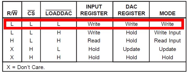
I would like to know the following status time chart of DAC7612E. -R/W:Low -CS:Low -LOADDAC:Low I attached Logic Truth table, I would like to get the time chart at red frame.
I'm not to sure what you mean by 'time chart', but page 5 specifies both the 'timing diagrams' and 'timing specifications' for the 14-bit data frame. Please let me know if this answers your question.
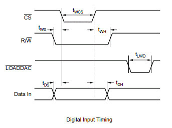
The following timing chart is the "Write Input MODE" timing chart of CS = L, R / W = L, LOADDAC = H, when I input the "Write MODE" of CS = L, R / W = L, LOADDAC = L, how do I input LOADDAC? Since tWCS and tLWD are the same 50 ns (min), should I input the waveform of LOADDAC same as wave of CS? Best Regards, Sho
The timing chart is displayed on page 5 of the DAC7612 datasheet. I've posted it below for reference. Please note that /LOADDACS refers to pin 3 of the same name. The timing specifications are displayed in the chart of the same page, please note that these timing specifications are minimums, so anything above is acceptable. Using the information on this page, we can conclude that the maximum clock frequency is 16.6MHz. The minimum data setup and hold is also shown to have a minimum requirement of 15ns each. Additionally, the /LOADDACS pin is shown to have a minimum load pulse width of 20ns.
The interface is further explained on page 10 of the DAC7612 datasheet. To summarize, the interface consists of four signals: SCLK, SDI, /CS and /LOADDACS. The /CS signal is brought low to initiate new serial communication by loading either DAC A or DAC B with new 14-bit serial data via the SDI input. /CS is then brought high, and latching is complete on the falling edge of /LOADDACS.
Please not that /LOADDACS must be returned HIGH prior to shifting in new serial data.
Sorry, the device name is typo. The device name that I would like to ask you is DAC7621E.
I write same question below
The following timing chart is the "Write Input MODE" timing chart of CS = L, R / W = L, LOADDAC = H, when I input the "Write MODE" of CS = L, R / W = L, LOADDAC = L, how do I input LOADDAC? Since tWCS and tLWD are the same 50 ns (min), should I input the waveform of LOADDAC same as wave of CS? So please tell me the response, sorry.
Thank you for the clarification. The timing diagram is as you posted, since this is a 12-bit parallel input DAC. The timing specifications again specifies the minimum timing constraints for each signal (It is generally common to include a pull-up resistor on active low signals such as /CLR, /CS, /LOADDAC).
The order of operation for a write is summarized in my sequence below:
It is generally good practice to condition the digital inputs before applying the /CS and R/W transition. This gives the digital inputs time to settle to their transient value.
Pull W/R pin to "LOW" from "HIGH" position
The datasheet specifies that a minimum time of 0 ns must elapse before /CS is brought "LOW". This would suggest that both the signals can transition in parallel.
The /CS must remain low for at least 50ns, anything above is acceptable.
There is a minimum R/W LOW after /CS HIGH that you must ensure, which is a value of 5ns. Therefore, you must make sure that R/W signal is brought HIGH before /CS is brought HIGH.The delta in transitions must be higher than 5ns.
To load the internal DAC registers, the /LOADDAC signal must be have a minimum active low duration of 50ns.
Please let me know if this answers your questions.
Thank your for your reply. I understood the timing diagram in datasheet.
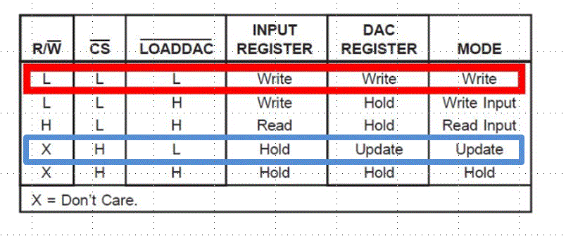
However, please check the red frame of logic truth table below. I can understand that if we pull /CS, R/W and /LOADDAC to Low from High, we can write to INPUT Register and DAC Register and the mode change to "Write mode" Please tell me the timing regulation of /DOADDAC in"Write Mode"?
Sorry, I would like to get your response as soon as possible, so could you please reply by 24th February ?
I believe I understand the question. The truth table does indeed display the logic levels to 'write' to the DAC Register, but this table does not necessarily state to use static voltages to achieve a write operation. The truth table must be used in conjunction with the timing diagrams displayed for correct device operation. Therefore to 'write' to a DAC Register please follow the procedure suggested in my previous post. As explained in the previous post, /LOADDAC signal must have an active low duration of at least 50ns, and this transition takes place after /CS and R/W signals are brought HIGH.
I have a question about your comment below. "As explained in the previous post, /LOADDAC signal must have an active low duration of at least 50ns, and this transition takes place after /CS and R/W signals are brought HIGH." I understood the /LOADDAC signal timing, but is the mode that teach me "update Mode"?(Blue Frame)
I think that I can write to DAC register and Input register directly in "Write Mode" So please tell me the write timing and regulation of /READDAC in "Write mode". I can understood /CS and R/W Low timing from datasheet, but I can't know the Low timing of ?LOAD DAC.(Red Frame) I'm sorry I have asked you many times.
The DAC7621 device includes a double-buffered register structure. This means that new data can be entered into the DAC without disturbing the old data and the analog output of the converter. At some point after the data has been entered into the serial shift register, this data can be transferred into the DAC register through a HIGH to LOW transition of the /LOADDAC pin. However, the /LOADDAC pin makes the DAC register transparent. If new data becomes available on the bus register while /LOADDAC is LOW, the DAC output voltage will change as the data changes. To prevent this, /CS must be returned HIGH prior to changing data on the bus.
Using this information with the truth table presented above we can understand that a write and update can either be accomplished by performing the action displayed in the red frame, or alternatively, you can break the sequence into two frames (one that updates the first buffer register, and the second latching the data into the second data register that results in updating the DAC). The sequence for this second option, is frame 2 and frame 4 (blue).
I have one question about the following your answer. "Using this information with the truth table presented above we can understand that a write and update can either be accomplished by performing the action displayed in the red frame" >>When I input the "Write MODE" of CS = L, R / W = L, LOADDAC = L, how do I input LOADDAC? Since tWCS and tLWD are the same 50 ns (min), should I input the waveform of LOADDAC same as wave of CS? If it is know plase tell me the LOW timing od /LOADDAC in "Write Mode"
Sorry, please give me your answer as soon as possible.
/CS and /LOADDAC cannot be connected together. As illustrated in the Digital Input Timing diagram in the previous posts or on page 4 of the DS, /LOADDAC must be asserted LOW after /CS is brought high. The /CS and /LOADDAC waveforms can have different active low durations, with a minimum duration of 50ns -- anything above 50ns is acceptable.
Therefore, for instance /CS can have an active low duration of 80ns, and /LDAC can have an active low of 60ns. Since both are above the 50ns minimum active LOW requirement, both are acceptable for normal operation.