This thread has been locked.

If you have a related question, please click the "Ask a related question" button in the top right corner. The newly created question will be automatically linked to this question.

ADS9110: ads9110

Part Number: ADS9110
Other Parts Discussed in Thread: REF5045, OPA625, , OPA378, THS4551

Hi, I am using 24 of ADS9110 ADCs on a board and would like to provide a common 4.5V reference to all (if not one for 12 devices). I'm planning follow the design based on REF5045 and OPA625 that is provided in the datasheet and provide 3 x 10 uF capacitors per ADC. The design is to be used at 2MHz sampling and I still want to achieve performance within 1LSB (3.8ppm x 4.5V = 17uV).

Can you please advice me if the reference circuit provided in the datasheet can reliabley work on this arrangement?

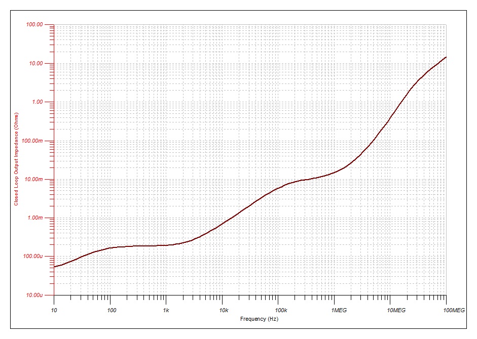
I have used TINA and simulated the reference circuit (REF5045+OPA378+OPA625) with 360uF capacitive load. I used a Iload of 15mA @ 2MHz and the ripple is about 21uV (approx.). Is this 15mA @ 2MHz an overhill to test the circuit? Is thts 2MHz the representation of CONVERION (i.e, the rate at witch the Iref is drawn)?

I am in the process of finalising the schematics and cannot make up my mind on this. The design is pused to give the optimum SNR and dynamic range.

I also want to have a separate buffer attached to the same reference IC REF5045 to generate VOCM (2.25V) for 24 sets of THS4551 fully differential amplifiers. Is this allowed or should I implement a separate circuit to avoild possible glitches?

I have included the TINA circuit that I simulated.

Thanks

Regards

Billy

  • Hello Billy,


     I will go ahead  and set up a model for this in TINA accounting for the transient current loads for the 12 ADS9110 driven by the composite amplifier (opa378+OPA625).  I suspect that you will not be able to drive all 12 ADC's at the same time using a single composite amplifier buffer. 

    Are these 12 (or 24) ADC's simultaneously sampling at 2MSPS?  If not, how many will be converting at the same time? or how are the conversions interleaved?

    Please allow a couple of days.


    Thanks and Best Regards,

    Luis

  • Hi Luis, thanks for your reply. The ADCs would sample data simultaniously at 2MSPS.
    I couldn't workout the exact output impedance of the composit amplifier circuit provided, but I can see it can be in the milliohm range. Can you tell me this value (is it 4.7 Ohm/acl)?

    When I loaded this composite circuit with 360 uF capacitor (TINA simulation) the simulation seemed to show steability. I also gather the OPA625 can output about 150 mA. I loaded the circuit with a 15mA@ 2MHz load and the performance was not well within 1LSB (that is about 17 uV in this case - 3.8ppm x 4.5V). Therefore I found it difficult to make my mind up.

    I also would like to include isolation resistors between the ADCs (on each brance) so that the action on one doesn't interfere with the other. But this can increase the output impedance of the buffer circuit and possiblyjeapadise the 1LSB performance. Do you think this is necessary to isolate the ADCs? I can allow foot print for this but not fit initially, but with the multiple channels it is cumbursome to fiddle with the components.

    Moreover the evaluation board for ADS9110 for some reason did not use this reference circuit.

    I also enquired if I can use the same reference with a separate buffer to provide VOCM to the diferential drivers (12/24 of them) without interfearing with the ADC performance.

    I will wait for your reply and thanks again fro this.
    kind regards
    Billy
  • Hi Billy,

    Attached is a quick TINA simulation of the closed-loop output impedance of the composite amplifier circuit and a plot of this impedance over frequency.

    Although the ADS9110 draws an “average” current of ~1.25mA while performing conversions at 2MSPS, the reference pin needs to be modeled as a dynamic load to the reference source where high current transients are present.   Since the reference voltage is sampled several times during each conversion, high-current transients are present where the ADC’s internal capacitor array is switched and charged as the bit decisions are made. The reference voltage must remain settled within the required N-Bit resolution during each conversion clock cycle, or linearity errors and missing code errors may occur; and should not droop during conversions.

    I am working on a simplified model of the ADS9110 REFIN transient current load in order to simulate in TINA the various ADC’s connected to the composite buffer and the transient response of the composite buffer to this load. I will also include in the analysis the approximate inductance/capacitance in the connections to estimate the effects of each ADC on each other.

    AC Stability analysis suggests the composite amplifier circuit is still stable with the additional bypass capacitive load, an effective 21uF (603 10V X7R 3x10uF) x 12 ADCs; although we may need to add a small (~100mOhms or so) series resistance with each ADC reference input to increase phase margin. I will need to look into this in more detail with the transient ADC load model.

    Using a separate voltage divider with RC filter and buffer to produce the VOCM should be fine.

    To the best of my knowledge, the ADS9110 EVM uses the composite circuit including the OPA378+OPA625 as a reference buffer. Please let me know if you have an evaluation board that does not include this circuit.

    I will provide you an update with the detailed transient simulations showing the settling soon and to let you know how many ADC’s can be driven with each composite buffer circuit.   I am in business travel this week but will be working in parallel on this case.   Please allow 1 week for the complete analysis.

    Thank you and Best Regards,

    Luis Chioye

    OPA378_OPA625_ZOUT_4-4-17.TSC

  • Hello Billy,

    I have performed an approximate simulation using a simplified reference load model for the ADS9110. Since the circuit involves several ADC’s, to avoid convergence issues of the complex circuit, I used a piecewise linear current source to emulate the transient currents present at the reference pin of each ADC.

    If one ADS9110 is driven by the composite amplifier, the reference voltage will droop around ~29uV (less than 1LSB) during the first set of conversions and then stabilizes to about 18uV droop.

    When two ADC’s are driven by the composite amplifier, the reference voltage will droop around ~47uV (or 1.4LSB) during the first set of conversions and then recovers to about 24uV droop.

    If 4 ADC’s are driven by the composite amplifier, the reference voltage will droop around ~63uV (or 1.8LSBs) during the first set of conversions and then recover to about 20uV droop.

    On the simulation, I assumed a solid plane on the top layer with very low impedance (~10mOhm) is used to connect the reference voltage to the REFP pins of all devices and the bypass 3x10uF+10nF local capacitors are placed in very close proximity to the ADC to reduce errors.

    The design will be very sensitive to PCB layout; therefore, for symmetry, I believe limiting the design to two or four ADC’s per composite buffer may be possible using a solid plane for the REFP and REFM connections. As more ADC’s are connected the droop could increase due to the transient response of the composite amplifier and due to the PCB parasitic impedance. For example, a 5 inch 25mil trace of 1-oz Cu could add up to 100mOhm trace resistance in the path and this would increase the droop to ~200uV.

    Please see attached the simulation files and let me know if you have any questions and/or if you have a schematic/layout that you will like us to review.

    Many Thanks and Best Regards,

    Luis Chioye


    Reference droop Simulations:

    Multiple_ADS9110_singlebuffer.zip