This thread has been locked.

If you have a related question, please click the "Ask a related question" button in the top right corner. The newly created question will be automatically linked to this question.

ADC3422EVM: Transformer Used in ADC Evaluation Modules

Part Number: ADC3422EVM

Hi All, 

we are interested in ADC Evaluation Modules ADC3442EVM, ADS6422EVM, and ADC3423EVM. However, we have some simple technical questions to confirm our choices are correct for our application. I was wondering if you let us know the answer of the following questions:

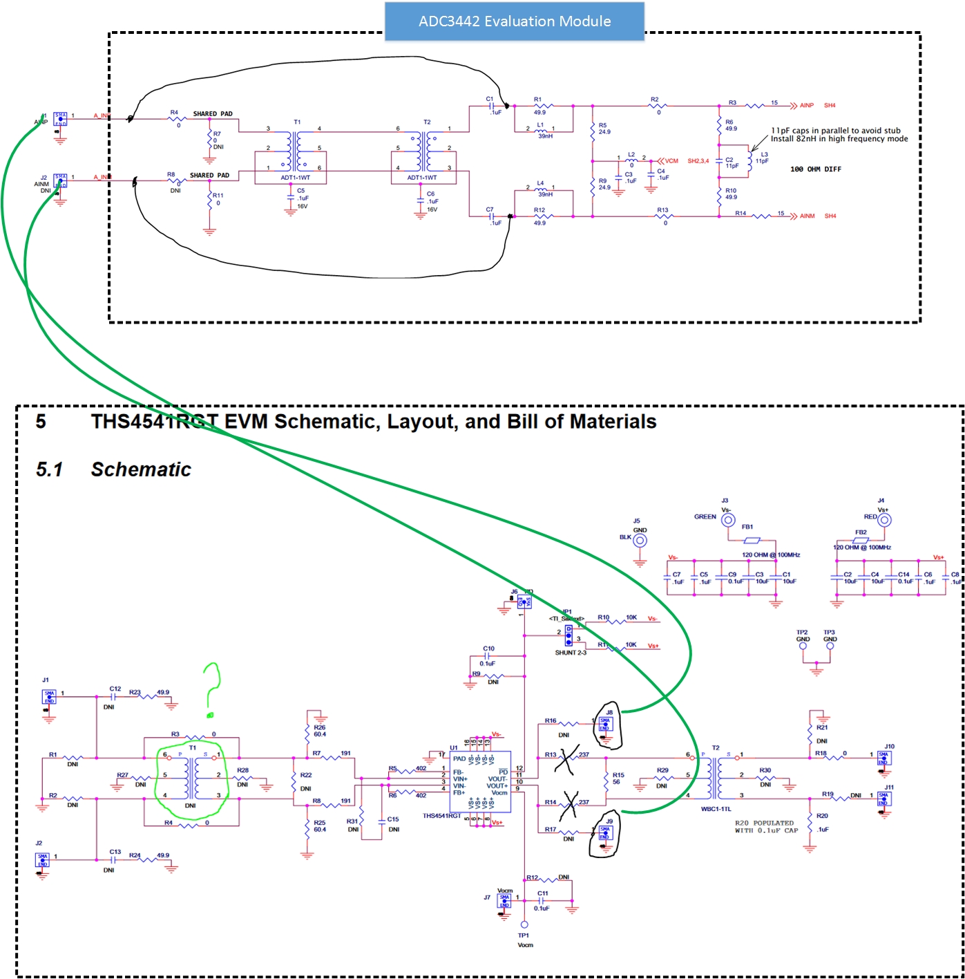
- I saw TI  uses 1:1 transformer for each analog input pin to have ac coupling. However, our analog signal is not a pure ac signal and has a dc bias which varies during time. So are our choices right for this application? In other words, does putting transformers in the path of analog signals impose any constrain for analog signals we can convert? for example, just pure high frequency ac signals can be converted by this evaluation kit.

- In order to capture the output digital converted data, we are using FPGA (Zedboard), which its input banks are compatible with LVCMOS data type. So we need to use ICs to converter LVDS data to LVCMOS, Is there any other option? 

- And the last question is that: considering conversion time, serializing the data, and capturing it inside the FPGA, what should be the minimum sampling rate of ADC if we want to have the data inside FPGA after 800 ns from start of conversion command?

Thank you

  • Hi Masih,

    Transformers in general are AC coupled - the DC component cannot pass through. In general the frequency response of the transformer can be considered a high pass filter with a corner frequency around 100kHz-1MHz (this will vary depending on the transformer). The transformer will pass AC signals, and will reject DC or low frequency signals.

    Unfortunately the ADC only has LVDS outputs and you will need to have an LVDS interface. The recommended evaluation platform is the TSW1400EVM. However you should also be able to get it working with any LVDS interface with some effort.

    The ADC is constantly capturing data at the clock rate. The output of the deserializer in the FPGA should be providing samples. It will be up to your implementation as to when you decide to collect the data - either based on some kind of trigger or some kind of interrupt or need from your system. Things like the sampling rate and latency of the ADC will only determine the total latency from when your signal gets to the ADC and when that sample appears inside the FPGA. The ADC latency is in the order of 8-9 clocks. If you want to see 1 sample after 800ns, this implies 9/800ns=11.25Msps.

    Ken.
  • Hi Ken,

    Thank you so much for your precious information. It was so helpful.
    I took a look at several ADC evaluation boards. It seems that all of them have ac-coupling for input analog signals. Can you suggest me a dc-coupling evaluation board or something else that can work for us.
    In fact, our signal is a triangular waveform at 50 kHz with a dc bias, which should be measured with at least 10 MSPS.

    Thank you,
    Masih
  • Hi Masih,

    Typically the ADC EVMs are designed with passive transformers in place to make it easy to do evaluation using test equipment such as a 50 ohm signal generator. The transformer provides a nice means to generate a differential signal into the ADC.

    For DC coupled applications you normally require some kind of amplifier interface to provide the SE to DE conversion. We normally recommend using some kind of Fully Differential Amplifier (FDA) for this application. Although we don't generally make EVMs for this kind of application, there is an example of this that may help.

    Are you planning on making your own board or using something ready made from TI? We don't have many EVMs ready made for this kind of application. However we do provide some reference design material that may be useful in developing your own system.

    www.ti.com/.../TIDA-00294
    www.ti.com/.../tidu500.pdf

    If you check the ADC EVM schematic you can see that there is a means to bypass the transformer and go out differential to the SMA connectors. In this case you may be able to connect this input from a FDA EVM such as the THS4541EVM.

    www.ti.com/.../THS4541RGTEVM


    Ken.
  • Thank you for your time and consideration Ken.

    I have attached the option in which ADC EVM transformer is bypassed, and THS4541EVM is used for SE to DE conversion. Is the bellow schematic what you mean?

    And I also should bypass the transformer at the input side of THS4541EVM, right?

    I really appreciate your time you allocated for my question. 

  • You have to also connect the common mode voltage from the ADC into the THS. See figure 3 of the TI Design
    www.ti.com/.../tidu500.pdf

    Ken.
  • Oh, right.
    Thank you Ken, it was a great help for me :)
  • Hi Masih,

    For DC coupled application, the input side transformer on the THS4541EVM should also be bypassed. You could either connect the common mode voltage from ADC to the THS, or use external 0.95V on the Vcom pin of the THS4541. The supplies on the THS4541EVM would need to be +3.5V and -1.5V so that the amplifier output swing is centered at mid-rail of 0.95V.

    Best Regards,

    Rohit