This thread has been locked.

If you have a related question, please click the "Ask a related question" button in the top right corner. The newly created question will be automatically linked to this question.

ADS1220: ADS1220: Measurement variation with Analogue supply

Part Number: ADS1220
Other Parts Discussed in Thread: , OPA314

Hi all,

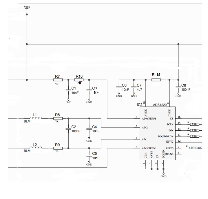
I am currently developing a load cell measuring device that will be battery powered. In order to reduce PCB real estate use and improve efficiency of the battery usage I am planning to take the analogue supply from the terminal voltage. Everything is communicating and measuring OK but I am having issues with the measurement stability with battery terminal voltage.

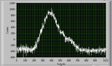
The measurement is ratiometric and as such I expected the measurement to self compensate as the analogue voltage changed. I am seeing variations of roughly 0.7 uV/V when changing the supply voltage between 3.5 V and 2.4 V. I have added the plot to show what I have observed.

Is there any data that characterises the variation of the measurement with analogue supply as I could not find anything specifically relating to this in the data sheet.

Is this characteristic typical of these devices.

Regards,

Clive.

  • Hi Clive,

    Welcome to the forum and thanks for looking at the ADS1220.  There is some degradation in the measurement relative to the supply voltage.  In the datasheet this is specified as PSRR.  As to your graph and explanation I'm not sure I completely follow your description.  It would be helpful for me to see your schematic, all register settings, and the raw data.  It would also be helpful to know the sensitivity of your load cell, weight limit and if any load is being supplied.

    Best regards,

    Bob B

  • Hi Bob,

    Many thanks for the quick response.

    Yes, I realised after I posted it that I was only really supplying half of the story. The schematic is essentially the same as the resistive bridge measurement example given I the datasheet (section 9.2.3). The main differences are that I have a first order filter on Ref P1 (matches RF2 and Ccm2) and the excitation and the analogue supply are taken from the battery voltage.


    The register settings are:

    reg0 - 0x3E

    reg1 - 0x94

    reg2 - 0x88

    reg3 - 0x00

    The highlights are that it is running at 660 Hz continuous mode with the PGA set to 128.

    The values that are shown are a direct conversion of the raw data to milli-volt per volt (raw data divided by 1073741.824). In the chart I am taking an average over a few hundred samples at each value of applied terminal voltage.

    The signal is provided from a load cell simulator set to -2.5 mV/V as such this doesn't change. The maximum input sensitivity on the adc in this configuration is +/- 7.8 mV/V.

    I had always thought of the psrr in relation to the noise ripple on the power supply rather than in relation to the absolute value of the supply voltage. I had expected the level of noise to increase slightly as the terminal voltage changed as the SNR is reduced but I was not expecting the change in the average value. Especially as it is a ratio-metric measurement.

    I will run through some numbers using the PSRR and see where that places me. If you have any suggestions please let me know.

  • Hi Clive,

    Thanks for the information.  I'm still not quite sure how you are actually applying your calculations.  It is always easier for me to think about the system performance relative to the raw code output.  The calculated output may be somewhat misleading as to what is actually happening. 

    Normally you would think of power supply rejection relative to AC rejection.  The DC change is essentially a very slow AC signal where only half of the cycle is being considered.  I looked into a DC code shift a couple of years ago with not quite the same setup.  Basically there are a number of issues going on.  When you change the AVDD voltage, the PGA will have a slight shift in offset error as well as gain error.  There are a couple of gain error plots in the ADS1220 datasheet (figures 5 and 6) which show gain error with temperature and at 2 different supply voltages.  As the PGA relates directly to the analog supply, the ratiometric measurement does not affect the PGA performance.

    I also just ran some more tests using a similar setup to your configuration with the ADS1220EVM.  Unfortunately the level shifters to the micro will not let me go below 2.8V.  One thing that I had not taken into account with my earlier tests is the affect of noise in the measurement.  In my previous tests I had used a constant reference voltage while adjusting AVDD.  I was also using a gain of 1.  I did not see the effect of noise in the measurement in those tests.

    For the ADS1220, the shorted input test gives the best case noise scenario for the ADC.  This is inherent to the conversion with little respect to the supply voltage.  In the datasheet we specify the noise using an analog supply of 3.3V.  When using a load cell simulator I was able to achieve the datasheet performance for noise.  If the noise stays roughly the same, but the reference value lowers, there will actually be an increase in the number of codes for noise.  Depending on the noise distribution during the collection period, there may be a shift even though the measurement is ratiometric.

    One other thing that might cause a slight error is the low-side switch. The resistance is quite low, but the resistance will increase slightly as AVDD decreases.

    When calculating your results, did you calibrate the ADS1220 first and account for offset and gain error?  What AVDD supply voltage did you use as the standard for calculation?  From my measurements I had a mean code value (512 samples) of 2687696 for 3.46V AVDD and for 2.86V code of 2687720.  Between the 2 supply voltages I see a difference of codes which is well within the level of noise.

    Best regards,

    Bob B

  • Hi Bob,

    I am at least glad to hear that when you tried it the performance was good. If I could get the change down to around 50 counts I would be happy.

    I have run through some of the things you raised in the last response. It doesn't appear to have anything to do with the power switch. I shorted between the AIN3/REFN1 and ground so as to remove any variation and the effect was the same.

    I have been trying several different data rates and configurations and this does have an impact. Really not sure why but the data for the original curve is:

    2.3 -2684301
    2.5 -2684526
    2.7 -2684752
    2.8 -2684623
    2.9 -2684081
    3.1 -2684027
    3.3 -2683914
    3.5 -2683887

    I have subsequently run some tests using a different data rate at 90 sps and the following results are obtained:

    2.5 mV/V
    3.4348 2684808
    2.9585 2684974
    2.6572 2685392
    2.43 2685914
    "-2.5 mV/V"
    3.4345 -2683121
    3.029 -2683121
    2.687 -2682619
    2.431 -2682447

    I should mention that the values given above do not have any averaging. This is just the raw value straight from the adc.

    I also tried splitting out the power supply. If I maintain Analogue Vdd at a fixed level and vary the supply to the rest of the board there is no problem. If I fix the supply to the main section of board and vary analogue vdd the change returns.

    I have also tried moving the feed point for the excitation to be at the same point as the analogue supply but I still have the same variation. I still don't understand how I can be getting a variation of up to 850 counts on the adc when you see 30.

    2.5 mV/V
    3.4348 2684808
    2.9585 2684974
    2.6572 2685392
    2.43 2685914
    "-2.5 mV/V"
    3.4345 -2683121
    3.029 -2683121
    2.687 -2682619
    2.431 -2682447
  • Hi Clive,

    Perhaps I wasn't clear in my previous explanation.  The results of the code difference was based on the mean of 512 samples.  The noise is actually quite high, so if you take any individual point you may see hundreds of codes variation to the next point.  Take a look at Table 5 in the ADS1220 datasheet.  The values in the table are based on shorted inputs where the value of the reference has little effect.  These numbers are the best case numbers.  Notice that at 660sps there is 2.93uV of peak to peak noise and at 90sps there is 690nV of noise peak to peak.  A single code for a 3.3V reference will have a value of approximately 3.1nV per code.  However, the value of 1 code for 2.4V will be approximately 2.2nV.

    From your data it is not clear as to what the mean value should be relative to the amount of code shift you are seeing.  The lower data rates of the ADS1220 have a similar affect as averaging.  The delta-sigma converter is an oversampling device that pushes the quantization noise into the higher frequencies then by decimation will filter the noise similar to a low-pass filter.  The higher the bandwidth the higher the noise.

    The code spread for the 3.3V reference and 2.93uVpp noise will be 953 codes at 660sps and will be 224 codes of noise for the 90sps.  At the 2.4V reference the code spread will increase due to the reduced reference value reducing the LSB size.  The code spread will now be 1310 codes and 308 codes respectively.  With Gaussian noise, the code shift can be rather substantial from the mean value.  By ratiometric measurement the mean code should stay relatively close throughout the supply range, but the actual values may deviate +/- 476 codes from the mean at 3.3V and as much as +/- 655 codes at 2.4V.  These results are based on shorted input and do not reflect any additional noise as a result of EMI/RFI or power-line cycle noise.

    I would suggest taking a large group of data to determine the mean at each supply voltage setting and then calculate the amount of shift from the mean from one voltage setting to the next.

    Best regards,

    Bob B

  • Hi Bob,

    I think I need to go back to the beginning on the data. I have set up my system to output data at 2 Hz. Each data point is taken with the adc running at 90 samples per second in continuous conversion mode. The micro is controlling the ADC and collating an average across 16 adc readings and transmitting them. After the 16 samples have been collected the the adc is placed in stop mode until the transmission period expires. My monitoring software is collecting this data and calculating an average and noise free bits from the measurement.

    I have collected the following two sets of data where 30 seconds of data is averaged (60 data points). The data transmitted from my board is noise free to within 50 adc counts. This is effectively an average across 960 samples at 90 samples per second.

    At -2.5 mV/V I obtain:

    3.398 -2682945
    3.035 -2682880
    2.708 -2682492
    2.405 -2682738

    At 2.5 mV/V I obtain:

    3.397 2685028
    3.042 2685182
    2.713 2685703
    2.44 2685758
    2.4

    2685687

    There seems to be a really strange feature in the data in and around 2.6 Volts. I have tried everything I can think of to try and remove it without success. I am really confused as to why the feature is different depending upon the applied input to the adc. I would have thought that an artefact like this would be the same no matter what the input is.

  • Hi Clive,

    When you say you place the ADC in 'stop mode', are you issuing the POWERDOWN command? If so, there may be some issues with analog settling on restart.  I also noticed on the schematic that you have a ferrite between AVDD and DVDD.  There is enough inductance in the ferrite that can starve the ADS1220 of needed current when powering up.  If you want to add some filtering between the DVDD and AVDD supply inputs I would suggest replacing the ferrite with a small value of resistance in the range of 1 to 10 ohms to act as a low-pass filter in combination with the capacitors C6 and C7.

    It may be possible that there is some offset shift in the PGA/modulator as the analog voltage changes.  You can check this by using the internal short to (AVDD-AVSS)/2 as the mux selection and see if this offset is shifting over voltage.

    For me to check this myself, I will have to modify my board to provide the power in the proper way so as not to affect the level shifters.  I will get to this as soon as I can, but it may take me a day or two.

    Best regards,

    Bob B

  • Hi Clive,

    I was able to vary the AVDD supply for the ADS1220 from 2.3 to 5V.  There is definitely a code shift within a certain voltage range relative to the input common-mode.  As the output of the load cell simulator is very close to (AVDD-AVSS)/2, the shift can be clearly seen when using the mux input selection of (AVDD-AVSS)/2.  This result shows there is the shift in the offset as the AVDD supply is varied.  The graph below shows the effect when I manually changed the AVDD supply voltage starting at 2.3V and ending at 3V.

    The effect is best explained in the OPA314 datasheet.  The explanation is on page 17 in section 7.3.2.  The ADS1220 uses a similar topology to achieve a rail-to-rail input.  The transition region is occurring at approximately 1.3V below AVDD, which is about 1.3V common-mode for a 2.6V AVDD supply.  That is why there is a deviation within that supply region of approximately 2.5 to 2.7V.

    So now we know there is a shift in offset within a particular region what can be done?  The easiest method would be to subtract the offset the same time as the measurement is taken.  This would require 2 sets of readings.  The first is by using the mux selection for the shorted input at (AVDD-AVSS)/2.  The second measurement is by changing the mux to the desired measurement channels and measuring that mux input.  The calculated results would be the measurement channel result subtracted by the offset.  This should give a much more consistent result over all AVDD voltages.  To maintain similar timing as you currently have you could take 8 samples and average for each measurement instead of the 16 you were using before.  Or you could do some other combination, like 4 samples at 0V input and 12 samples with the desired measurement.

    Best regards,

    Bob B

  • Hi Bob,

    That's great. I am very glad that this can be explained and there is a way around it. I still haven't decided how to efficiently code this in firmware but I did run some tests yesterday and it got me down to within 0.2 uV/V across the supply range. This is sufficient for my purposes.

    Can I suggest that it might be worth adding a section in the datasheet that outlines the measurement of the offset if you are not using a fixed analogue vdd supply and perhaps the information you outlined from the OPA314 datasheet.

    I think there is also another linear element with supply voltage which if I implement will get me down to 0.05 uV/V.

    Many thanks for your help.

    Clive.

  • Hi Clive,

    This won't help you specifically because of the mux input you are using, but it was suggested to me by one of my colleagues that the offset can also be removed by swapping the inputs via the mux to reverse the input polarity (of AINP and AINN) and thus creating a chopping of the offset by averaging the two results.  This may be helpful for someone reading this thread that can possibly use an input combination where they can swap the inputs via the mux. 

    Best regards,

    Bob B