This thread has been locked.

If you have a related question, please click the "Ask a related question" button in the top right corner. The newly created question will be automatically linked to this question.

ADS1014: Differential Mode and Full Scale Range

Part Number: ADS1014
Other Parts Discussed in Thread: ADS1013

I'm not quite understanding full scale range and its bearing upon differential versus single-ended mode for the ADS1014.


1) Full scale range is specified as +/- n volts.  However we cannot go below the supply voltage ground reference.  So, is FSR applicable to differential mode only?

2) The high range +/- 6.144V has a 3mV resolution.  If I consider +/- 6.144V to mean a span of 12.288V, then 12.288/.003 == 4096 bits, and we use them all.  However, as we cannot go negative, what then does +/- 6.144 mean?  Perhaps differential mode allows the full span of each range to be used?    

3) In single-ended mode do we connect AIN1 to GND? I don't see any advantage to put a positive bias on AIN1.

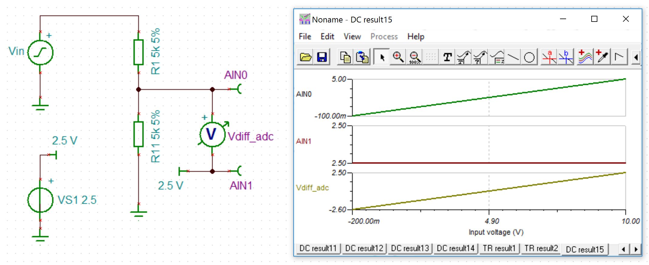
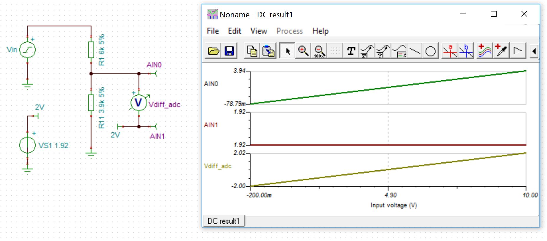
Our practical problem is this: we need to measure a sensor that tracks from -0.2v to +10V.  Starting with a +/- 0.256V FSR, will changing the range as the signal rises be a good option?  For a jellybean 10 bit ADC (+3V) we've processed the signal so the sensor voltage span translates from 0 to 3V.  In doing so we lose quite a lot of resolution.  Perhaps the ADS1014 offers us a better way?


  • Dear K1mgy, 

    1) You are right. Each input signal can´t go below GND, but in the case where AN1 has a higher input signal than AIN0 the differential signal becomes negative (Differential signal = AINO-AIN1). In single-ended signal mode, you can only use half of the full-scale range.

    2) The calculation of the resolution looks right but I recommend you have a look at Table 7.3 (Recommended Operating Conditions) in the datasheet. The recommended maximum Input signals, V(AINx),are limited by VDD which has a maximum of 5.5V. Therefore the full span of differential signal is ±5.5 V.

     3) ADC offers the highest accuracy by a common mode voltage around mid-supply (VDD/2). Therefore both input signals must shift by a bias VDD/2. Differentially, the signal will be centered around 0V, which allows you to use the full-scale range.

    If I understand your question correctly, I suggest you change the FSR depending on the level of the input signal. This will help if you need a higher resolution at a lower voltage level.

    To get the best resolution I would recommend to translate the signal in the span from 0-2V, which is completely covered by the FSR of 2.048 V.

    Feel free to upload your schematic for a review.

    Best regards,
    Florian

  • Florian thanks for the very helpful description.

    So,  if I convert my single ended adc driver to a dual ended,  where 0v in is presented as +1.25 v to the non inverting input and -1.25v to the inverting input, plus select the 2.048v FSR, then I'm not sure using an ADC with a PGA is a good choice.  I'll never be able to use the lowest FSR, correct?

  • Dear K1mgy,

    If the input signal at AIN0 is shifted by 1.25 V and AIN1 is connect to 1.25 V, the differential signal is equal to the input signal and only this span has to be covered by the FSR.
    But I have some really good news for you. The device will still work with a negative input signal close to GND. This means you don’t have to shift the signal up. Just reduce the signal via voltage divider to meet the full-scale range you choose.

    regards,
    Florian
  • If the input signal at AIN0 is shifted by 1.25 V and AIN1 is connect to 1.25 V, the differential signal is equal to the input signal and only this span has to be covered by the FSR.

    This technique might eliminate this op-amp-based level shift:

    I haven't adjusted this circuit for the present case.. but that's relatively easy.

    The device will still work with a negative input signal close to GND. This means you don’t have to shift the signal up. Just reduce the signal via voltage divider to meet the full-scale range you choose.

    I'm not so concerned with this given the level shift and offset, plus the differential mode.

    Here's a stock single-to-differential circuit.  I believe this will give the advantage of the common mode rejection and (with a little tweaking) work within the ADC input span.  

    Any thoughts on this technique?

    Note that the sensor is a very slow integration amplifier.  We're measuring 30 seconds of Dv/Dt.  Good to have millivolt resolution where possible throughout the entire span.

    Given the combo of the level shift and differential conversion, is it appropriate to start at the highest ADC PGA gain and step towards the 2.048V FSR?

  • Thank you for sharing the schematic, that helps me see your needs clearly.

    To understand your schematic I simulated it on TINA TI and attached the file for you. As is, the circuit does not run correctly. I found the following issues:

    • Voltage divider R801 and R805 (Voltage shift is 30mV, but you need 200 mV)
    • Voltage divider ratio between R804 and R806 is changed with R11 in parallel with R806.
    • Instead of connecting AIN1 to the output of U4.1, it should be connected to the common-mode voltage of AIN0, such that:
      • (Vdiff = AINO - AIN1 = Vsignal+2.5V – 2.5 V= Vsignal)

    To simplify the circuit and reduce the footprint, you can combine the level-shifting and common-mode voltage setting to the mid-supply voltage in one stage.

    But let me show you two potential solutions, maybe it can be helpful for you:

    First one is the simple single-ended measurement with AIN1 = GND. The signal gets reduced by 4/10 voltage divider and can get measured with the FSR of 4.096 V. The LSB of the ADC is 4.096V /215 = 0.125 mV and the input signal (-0.2V – 10V) will be measured with a resolution of 0.125mV*10/4=0.3125mV.

    The next circuit is a pseudo-differential measurement with AIN1 = VCM. The voltage divider reduces the signal by 3.9/9.9. AIN1 has to get connect to 1.92 V, which is the VCM (VCM=V1 - V2/2 = 3.94 V-(-0.079 V))/2=2 V minus the 80 mV shift.

    The differential signal Vdiff_adc is in the range of ±2 V and get perfect covered by full-scale range of ±2.048 V. The LSB is 2.048V /215 = 0.0625 mV, which gives a resolution of 0.0625 mV*9.9/3.9 =0.16 mV for the input signal (-0.2V – 10V).

    The second benefit is that the common mode voltage close to mid-supply, which offers higher accuracy.

    Notes: Both examples are built for a VDD of 5V

  • Florian, the effort you put in to bring these ideas is extraordinary.  Thank you kindly.

    I thought it would be necessary to drive the ADC with a balanced driver.  Clearly this is not true.

    I see that a better understanding of this ADC would help me a lot.  As it is, your second solution offers the best performance.  I may want to add a non-inverting buffer before the ADC, but otherwise it looks great.

    Given the resolution of 160uV per bit, maybe the use of the PGA is unnecessary?  In such case, I might switch to an ADC that offers the same differential input and performance without the PGA.  Can you suggest something suitable?  I might also consider using an SPI bus, rather than I2C, but for now the I2C is OK.

  • It is a pleasure to me to be able to support you.

    I just noticed,that the screenshot I posted for the second solution is not the right one. Here the correct schematic and plot:

    We have the ADS1013 device, which has the same performance like the ADS1014, but without the PGA. The good thing is, that the fixed FSR of 2.048 V fits great in you application.