This thread has been locked.

If you have a related question, please click the "Ask a related question" button in the top right corner. The newly created question will be automatically linked to this question.

AMC1304M25: Only positive measurement range for AMC1304M25 or AMC1301

Part Number: AMC1304M25
Other Parts Discussed in Thread: AMC1301, , OPA376

Hello everybody,

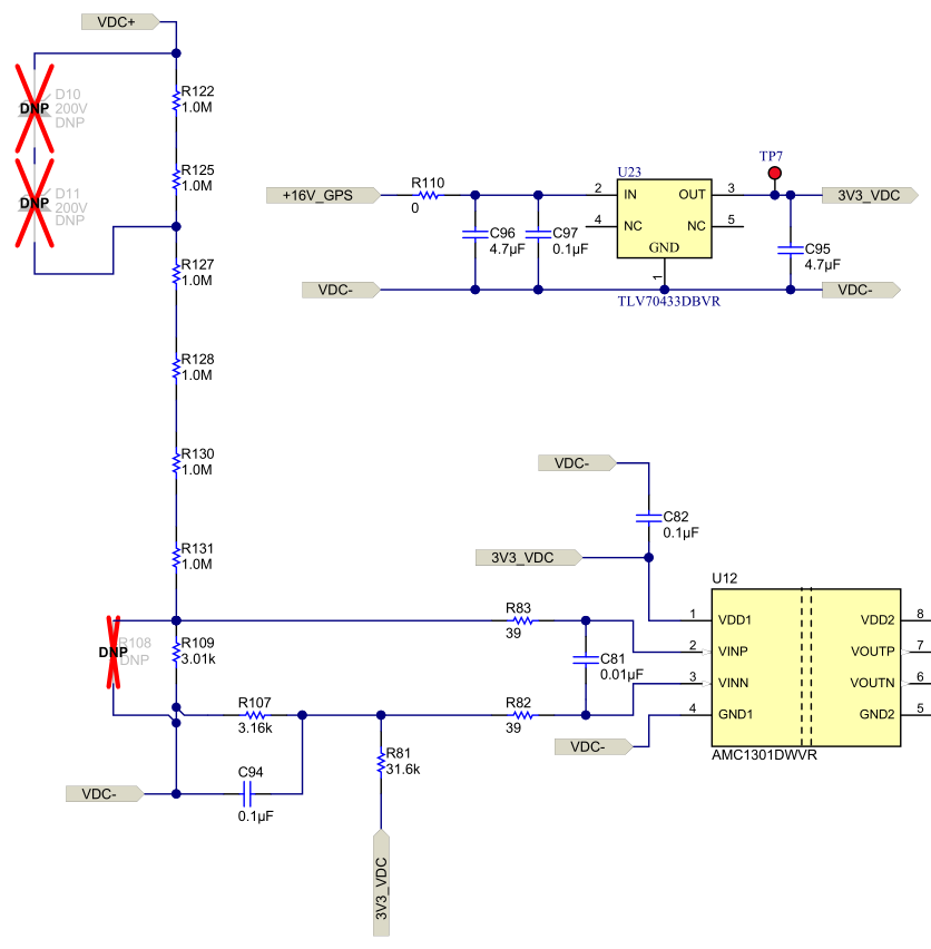
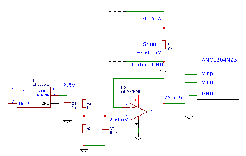
I'm planning to use the AMC1304M25 or AMC1301 for a isolated shunt-current measurement on the high-side.

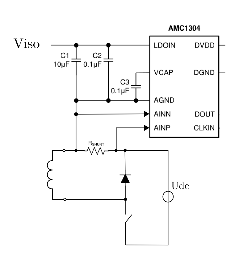
In my application, the current to be measured is only positive. Since the above devices have a differential input range of +-250mV, I was wondering if there is any way to modify the circuitry in order to have the range 0--250mV as linear full scale range for the digital conversion. Otherwise, I would be losing half of the measuring range. 

I would appreciate your thoughts on this.

Thank you,

Sebastian

  • Hi Sebastian,

    If you can get a little DC bias to your input, you can have the full dynamic range of the AMC1304 or the AMC1301. You just need to observe the common mode input voltage limitations of the respective device. For the AMC1304 the operating common mode input range is 1.2V. For the AMC1301, it would be VDD1 - 2.1V.
  • Hello Tom,

    Thanks for the reply.

    I was looking at the application note TIDUBX1B, specifically Figure 14, that is, using the AMC1301 for voltage measurement.

    I was wondering if one could use the same approach here for the shunt current measurement, adding a bias with the resistors R81 and R107 in order to better use the measuring range of the AMC1301.

    Is there anything special, that I have to consider in doing so?

    Regards, 

    Sebastian

  • Hi Sebastian,

    From the input perspective to the AMC1301 or AMC1302M25, it's still a voltage measurement, so there really is no difference. For the TIDU document, since the 'shunt' is large (3.01 k), there is some compensation taking place with the use of R107 and R81 (see voltage monitoring discussion in the AMC1301 datasheet, page 23). When using a low value shunt (sub ohms typical), putting a voltage divider in circuit like the one shown above will also cause some offset and gain errors, so it would be better to use a low impedance source - a buffer perhaps - to add the bias.
  • Hello Tom,

    yes, thank you for the comment. As also explained in TIDUBX1B (Sec 4.5), the resistor are used to compensate for the large shunt and to add an offset to VINN. For those of you, who would like more information about it, this is explained in detail in the application report SBAA215.

    In SBAA215, it is proposed to use the OPA376 to minimize the gain and offset errors. So, having this in mind, I planning to use the circuit below to add a 250mV offset to VINN, so that the differential voltage VINP-VINN changes between +250mV and -250mV, when the voltage drop in the shunt changes between 0V and 500mV. 

    What do you think, is this an adequate approach?

    Kind Regards,

    Sebastian

  • Hi Sebastian,

    With VINN at 250mV, there should not be any issue with swinging VINP from 0-500mV. What does your load look like?
  • Hello Tom,

    The shunt is placed in series with an inductive load as in the circuit of my first post above. Does this make a difference?

    Regards,

    Sebastian

  • Hi Sebastian,

    It was more a question out of curiosity than anything else.
  • Hello Tom,

    ok, thank you for the feedback.
    I think my original question is already answer.

    Regards,
    Sebastian