This thread has been locked.

If you have a related question, please click the "Ask a related question" button in the top right corner. The newly created question will be automatically linked to this question.

ADS8320: ADS8320

Part Number: ADS8320
Other Parts Discussed in Thread: ADS7056

Currently, I am working on a project where I’d like to use the ADS8320 A/D convertor. The only remaining open issue is the choice of reference voltage. Therefore I have some questions regarding the ADC behavior to reference noise which I hope you can help with:


    1. If the reference noise also contributes (with a scale factor) on the ADCs analog input, can it be said that both noise influences (analog input and reference voltage input) are partly correlated and thus partly cancel each other? Or is this wrong because both acquisition phase and conversion phase happen in different clock cycle so they are not correlated at all?


    1. If both noise contributions are uncorrelated, what is the worst case noise contribution of the ADC reference voltage input? Some sources tell me that the RMS reference noise will fully contribute to the total noise (if ADC is used full-scale) while other sources say only 40% will... Does this depend on which SAR architecture/switching method is used or can you clarify the ADC behavior for this noise source for me? Because the tight noise spec for this project it’s important for me to predict the worst case behavior of the ADC.

  • Hello Jan,

    1. When using independent circuits for driver amplifier and reference drive circuit, their noise will be uncorrelated.  Since these are different components in the signal chain, their contribution is treated as uncorrelated noise.  The combined noise contribution of the reference and input driver in RMS volts can be added by performing the square root sum of the squares (RSS)  to estimate the noise of the system. In a SAR ADC, the sampling of the input signal occurs at the end of acquisition period.  The SAR ADC reference voltage is sampled several times during the conversion period, as the bit decisions are made during the conversions process.

    2.  Since the RMS noise contribution of the input driver and reference driver are constant, the total noise of the analog front end can be estimated in RMS volts using the RSS operation.

    The SNR is the measured ratio of signal-to-noise at the output of the ADC. The signal is the rms amplitude of the fundamental and the noise is the sum of all non-fundamental signals up to half the sampling frequency fs/2, excluding dc and harmonics in the FFT. The SNR on a SAR ADC is specified for signals with amplitudes very close to full scale (typically -0.5dB to -0.2dB from full-scale).  Therefore, if the input signal decreases in amplitude, the SNR performance will degrade.  Although the noise contribution of the driver and ADC remains constant, the ratio of signal to noise has been reduced.

    Please find below a link on TI Precision Labs for SAR ADCs that discusses the topic in detail.

    https://training.ti.com/ti-precision-labs-adcs-calculating-the-total-noise-for-ADC-systems

    Best Regards,

    Luis


  • Hello Luis,

    Thank you for your fast response!

    Altough, isn't the noise contribution of the reference dependent on the ratio of the DAC capacitor divider internally? My measurements seemed to show that the total RMS output noise of the ADC increased with increasing output code? It could be however that I forgot to take something in account...

    Best regards,
    Sven
  • Hi Sven,

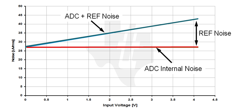
    The input referred noise of the ADC (in uVRMS) or the standard deviation of the ADC output codes remains constant regardless of input voltage or code; in other words, the noise and resolution of the ADC is fixed across the range.  In general, the designer needs to choose a low noise, low drift reference voltage and reference buffer circuit where the noise contribution of the reference does not degrade the performance of the SAR ADC. 

    If the noise at the reference driver circuit is larger than the noise specification of the ADC, then the ADC resolution will be limited to the noise of the reference across all codes. as the input signal voltage reaches full-scale. Below is a plot of the reference voltage noise contribution across input voltage.

    When testing noise on ADCs, it is important to use a very low noise sources.  When measuring the ADC SNR using a sinusoidal source, the user must ensure that the signal generator and input amplifier driver have at least 10-20dB better noise performance than the ADC under test.  The same concept applies when using a DC source, the noise of the DC source circuit must be lower than the ADC under test.

    Thank you and Best Regards,

    Luis


  • Hi Sven,

    Please see above, I have corrected/updated the previous post.  

    I general, we design the reference and reference buffer driver so their noise contribution is below the ADC internal noise.

    However, in the case where the reference noise is larger than the internal ADC noise, the reference circuit noise will dominate at voltages or codes close to full-scale.  Please see plot below.

    Many Thanks and Kind Regards,

    Luis

  • Hello Luis,

    Thank you very much for your clarifying update!

    All the components for this project need to be less then 500um thick (regular package or KGD). On top of this, there are tight constraints conserning noise and power dissipation. Therefore, the product range from wich we can choose is minimal. To get a decent comparision which of the reference will perform best, it's very helpful to fully understand this behavior. Knowing that this effect needs to be taken into account will definitely affect my choise!

    Kind regards,

    Sven

  • Hi Sven,

    What is the noise target in uVRMS or the resolution required?  We also have the ADS7056 is a 14-B 2.5MSPS ADC available on the X2QFN 1.5x1.5mm package with a thickness of 400um. It is ultra low power consumption, it consumes only 158uW when operated at 100kSPS:

    http://www.ti.com/lit/ds/symlink/ads7056.pdf

    The REF33XX is a 3.9uA, 30ppm/C available on the uQFN-8 1.5x1.5um.  Package thickness is slightly above the spec:  600um max thickness.

    http://www.ti.com/lit/ds/symlink/ref3325.pdf

    Thank you,

    Kind Regards,

    Luis