This thread has been locked.

If you have a related question, please click the "Ask a related question" button in the top right corner. The newly created question will be automatically linked to this question.

ADS4249: about OFFSET

Part Number: ADS4249

Hi all,

When the sampling rate is 180Msps and this is no signal input , there is some DC offset level without offset correction as below.

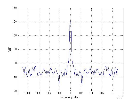
When increasing the input signal level of 140 MHz, a phenomenon in which the spectrum level at 0 Hz increases separately from the signal appearing at about the original 40 MHz was observed.
Why does this happen?
I think the offset level is the almost constant, isn't it? 

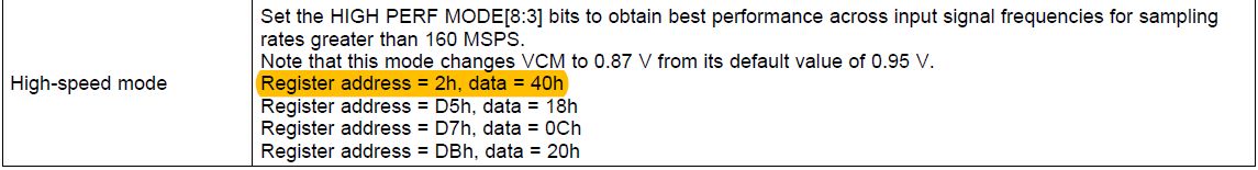
And when I want to reduce the this DC offset, Is it correct to set the registers as follows?

    Reg 0x3D = 0x20
       Reg 0x42=0x08   
       Reg 0xCF=0x00

  After completing the offset correction,  for freezing the offset pedestal, Reg 0xCF is set to 0x80.
  Is it correct?


Regards,
Toshi


  • Hi all,

    I have additional questions about ADS4249 register setting.

    ADC4249 input circuit is almost the same as EVM one's.
    In order to find the cause of the offset voltage, the voltage of VCM was 1.16 V when measured. But in the explanation of the datasheet, setting High Speed mode will cause VCM to change from 0.95 V to 0.87 V.

    After investigating why it becomes a value of VCM which is different from explanation with datasheet, the voltage of VCM was set to 1.16V by writing 0x40 to Reg 0x02.

    Why did you set the voltage of VCM to 1.16V?

    Anyway, I would like to add some information on the case of large offset.
    When OFFSET CORRECTION is set to FREEZE and Ach's PEDESTAL is set to Midcode + 31, the spectrum waveform becomes as follows.
    The three waveforms were captured under identical conditions.

     The register setting procedure is as follows; (In case of no offset correction) 
     Is there any problem with the setting order and content?

    Setting order   Address     Data
    1                        0x00         0x02
    2                        0x01         0x00
    3                        0x03         0x00
    4                        0x25         0x00
    5                        0x29         0x00
    6                        0x2B         0x00
    7                        0x3D         0x20
    8                        0x3F         0x00
    9                        0x40         0x00
    10                      0x41         0x00
    11                      0x42         0x08
    12                      0x45         0x00
    13                      0x4A         0x00
    14                      0x58         0x00
    15                      0xBF        0x7C
    16                      0xC1        0x00
    17                      0xCF        0x80
    18                      0xEF        0x00
    19                      0xF1        0x00
    20                      0xF2        0x00
    21                      0x02        0x40
    22                      0xD5       0x81
    23                      0xD7       0x0C
    24                      0xDB       0x20

    If you have any other question, please let me know.

    I am expecting an immediate reply.

    Best Regards,
    Toshi


  • Hi Toshi,

    We are taking a look into your questions, and will be back with you soon.

    Best Regards,

    Dan
  • Hi Toshi,

    Please see my below captures of before/after DC Offset is applied. Fs = 180MHz, Fin = 0 Hz.

    Before (approximately - 45 dB)

    After (approximately - 63 dB)

    I would write:

    0x00 0x02

    0x00 0x00

    0x44 0x01 (Enable Digital Function)

    0x3D 0x20 (Enable Offset Correction)

    I am still working on your other questions, and will get back with you soon.

    Happy Holidays,

    Dan

  • Hi Dan-san

    Merry Christmas!

    Thanks for your support.

    I am looking forward to receiving the answer as soon as possible.

    Best regards,
    Toshi 

  • Hi Toshi,

    I believe that the datasheet is incorrect since when I measured the default VCM (High-Speed mode not enabled) at 0.87V. When I enabled High-Speed mode, I saw the VCM jump to 0.95V. Intuitively, this also makes more sense.

    I think that the VCM might be set to 1.16V in order to get even faster clock transitions (low-high high-low), so I would use this setting if you are going to use High-Speed mode. If you are interested in power savings, you may want to tweak the VCM level and see how it effects performance in your design.

    In regard to the offset, I did not get the same results that you showed. I took several captures, and each one was relatively similar.

    The biggest difference I saw was when I adjusted the offset value to 31.

    The registers that you are writing look ok. Here are the register settings that I used for Offset Correction enabled(offset set to 0).

    x00 x00
    x01 x00
    x03 x00
    x06 x00
    x25 x00
    x29 x18
    x2B x00
    x3D x20
    x3F x00
    x40 x00
    x41 x00
    x42 x00
    x44 x01
    x45 x00
    xBA x00
    xBF x00
    xC1 x00
    xCF x80
    xD5 x00
    xD9 x00
    xDB x00
    xDC x00
    xEF x00
    xF1 x00
    xF2 x00

    Please let me know if I can help any further.

    Best Regards,

    Dan